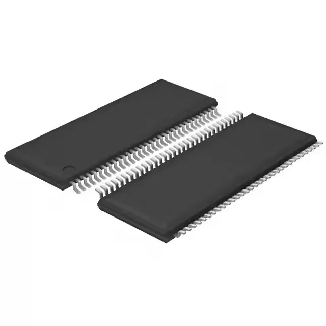
Texas Instruments SN65LVDS117DGGRG4 — Interface & Transceivers

SN65LVDS117DGGRG4 LVDS Buffer Multiplexer, 400 Mbps

MPNSN65LVDS117DGGRG4
Obsolete

Texas Instruments SN65LVDS117DGGRG4, LVDS Buffer/Multiplexer, 1 x 2:16, 400 Mbps max data rate, 2.8 ns delay, 3V–3.6V supply, 85 mA supply current, -40°C to 85°C, 64-TSSOP.

Independent supplier — new & surplus stockAuthenticity-screened · ESD-safe packingListing updated Jul 2026

Specifications

SN65LVDS117DGGRG4 specifications
ParameterValue
TypeBuffer, Multiplexer
MountingSurface Mount
Supply voltage3V ~ 3.6V
Current - supply85mA
Operating temperature-40°C~85°C
InputLVDS
OutputLVDS
PackageTape & Reel (TR)
Delay time2.8ns
Case64-TFSOP (0.240\", 6.10mm Width)
Data rate400Mbps
Channels1 x 2:16
Capacitance - input5 pF

Product details

What this LVDS buffer/multiplexer does

The Texas Instruments SN65LVDS117DGGRG4 is a 1 x 2:16 LVDS buffer and multiplexer. It takes one LVDS input and fans it out to sixteen LVDS outputs, or selects between two input banks. This part is used in high-speed backplane routing, clock distribution, and data fan-out where signal integrity over twisted-pair or PCB traces matters. The 400 Mbps maximum data rate and 2.8 ns propagation delay set the timing budget for the link.

TI no longer manufactures this specific variant.

The 400 Mbps data rate per channel is the headline number — it tells you the maximum serial bit rate the LVDS outputs can sustain. For a 16-output fan-out, the aggregate throughput is 6.4 Gbps, but each output still runs at 400 Mbps. The 2.8 ns delay time matters for clock skew budgets: if you are distributing a 100 MHz clock, that 2.8 ns adds directly to the total skew between the input and the farthest output. The 5 pF input capacitance is low enough that a single LVDS source can drive the input without a repeater.

The SN65LVDS117DGGRG4 comes in a 64-TFSOP package (0.240", 6.10 mm width), also referred to as 64-TSSOP in the supplier device package field. It is a surface-mount, fine-pitch package — the 0.5 mm pin pitch typical of TSSOP-64. The G4 suffix indicates a lead-free, RoHS-compliant finish. For layout, the 64-TSSOP footprint is standard; decoupling capacitors near each supply pin pair are recommended, though the exact count depends on the board stack-up.

Frequently asked questions

What is a direct replacement for SN65LVDS117DGGRG4?

No official TI successor is listed for the SN65LVDS117DGGRG4. The base product number is SN65L, and the closest functional sibling in the same family is the SN65LVDS117DGGR (without the G4 suffix), which differs only in lead finish (non-RoHS). For a pin-compatible replacement, the SN65LVDS117DGG (TSSOP-64, LVDS buffer/multiplexer, 400 Mbps) is the same die in the same package — verify the lead-free requirement against your assembly process. If you need an active-production alternative, look at the SN65LVDS117 series from TI or a cross from a second-source LVDS fan-out buffer family.

Is SN65LVDS117DGGRG4 obsolete?

Yes, the SN65LVDS117DGGRG4 is listed as obsolete. TI no longer manufactures it. For production needs, source through independent distribution against an RFQ.

What is the data rate of SN65LVDS117DGGRG4?

The maximum data rate is 400 Mbps per LVDS channel. This is the serial bit rate the device can sustain on each of its sixteen outputs.

What package is SN65LVDS117DGGRG4 in?

It is in a 64-TFSOP package (0.240", 6.10 mm width), also called 64-TSSOP. Surface-mount, fine-pitch (0.5 mm typical).