What this LVDS buffer/multiplexer does on your board
The Texas Instruments SN65LVDS117DGG is a 1:16 LVDS buffer and multiplexer that takes one or two LVDS inputs and fans them out to sixteen LVDS outputs. It is designed for clock and data distribution in high-speed serial backplanes, telecom line cards, and test equipment where signal integrity over multiple destinations matters. The 2:16 mux topology lets you select between two input sources, useful for redundant clock paths or switching between primary and backup data streams without an external mux.
Each output channel supports a maximum data rate of 400 Mbps, which is sufficient for LVDS links running at 400 MHz clock rates or lower-speed parallel busses. The 2.8 ns propagation delay (typical) adds a fixed latency that must be accounted for in source-synchronous clocking schemes — if you are distributing a 200 MHz clock to sixteen loads, the 2.8 ns delay is the same for all paths, so skew between outputs is minimal. Input capacitance is 5 pF, which is low enough that the upstream driver does not see a heavy load even when the mux is switching between sources.
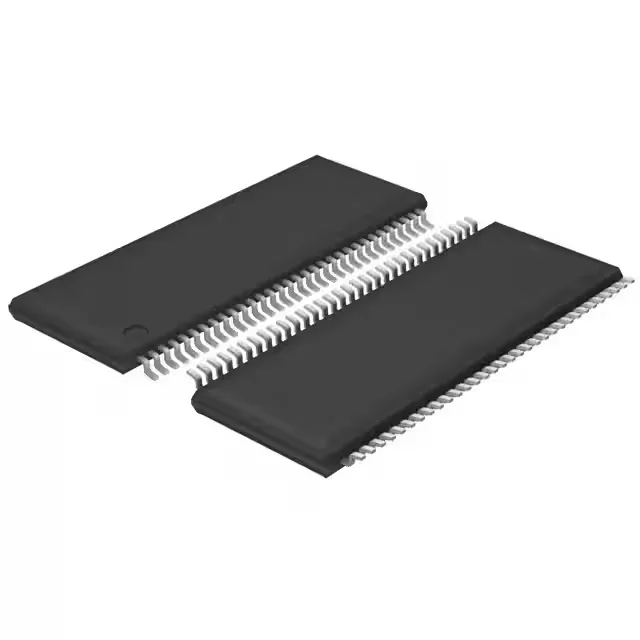
The SN65LVDS117DGG comes in a 64-pin TSSOP (TFSOP) package with 0.240" body width and 0.65 mm pitch. The supplier device package is 64-TSSOP. It is a surface-mount part, so standard reflow profiles for TSSOP apply.