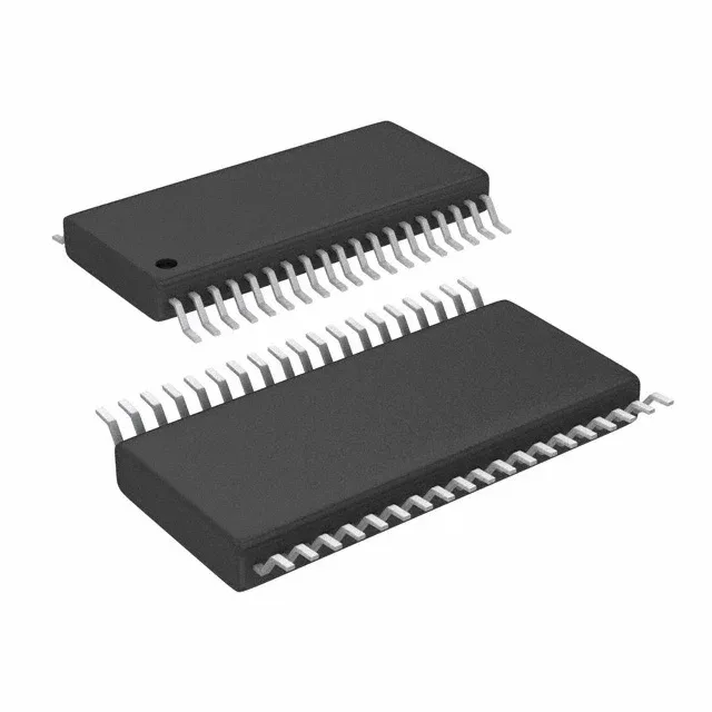
Texas Instruments SN65LVDS109DBTG4 — Interface & Transceivers

SN65LVDS109DBTG4 LVDS Buffer Multiplexer, 400 Mbps, 38-TSSOP

MPNSN65LVDS109DBTG4
End of Life

Texas Instruments SN65LVDS109DBTG4, LVDS Buffer/Multiplexer, 1 x 2:8 configuration, 400Mbps data rate, 2.8ns delay, 3V~3.6V supply, 46mA supply current, -40°C~85°C, 38-TFSOP (0.173", 4.40mm Width).

Independent supplier — new & surplus stockAuthenticity-screened · ESD-safe packingListing updated Aug 2026

Specifications

SN65LVDS109DBTG4 specifications
ParameterValue
TypeBuffer, Multiplexer
MountingSurface Mount
Supply voltage3V ~ 3.6V
Current - supply46mA
Operating temperature-40°C~85°C
InputLVDS
OutputLVDS
PackageTube
Delay time2.8ns
Case38-TFSOP (0.173\", 4.40mm Width)
Data rate400Mbps
Channels1 x 2:8
Capacitance - input5 pF

Product details

Active 1:8 LVDS fanout buffer/mux for backplane and clock distribution

The Texas Instruments SN65LVDS109DBTG4 is a 1 x 2:8 LVDS buffer and multiplexer in a 38-pin TSSOP package. It takes one of two LVDS input pairs and fans out to eight LVDS output pairs, with a maximum data rate of 400 Mbps per channel and a typical propagation delay of 2.8 ns.

400 Mbps per channel — what the rate means for the link budget

The 400 Mbps data rate is the per-channel ceiling for NRZ signalling. At this speed, the 2.8 ns propagation delay contributes roughly 1.1 UI of skew budget — a factor when daisy-chaining multiple fanout stages or distributing a clock across a backplane. The input capacitance of 5 pF loads the upstream driver; a source with 50 Ω output impedance and 3.3 V swing will see a 250 ps edge-rate degradation from this load, which is manageable below 400 Mbps but tightens margin at the upper end.

The base product number 65LVDS109 spans multiple package and temperature variants, but this DBTG4 suffix (38-TSSOP, RoHS) remains the standard production code.

Frequently asked questions

What is the data rate of SN65LVDS109DBTG4?

The maximum data rate is 400 Mbps per LVDS channel. This is the NRZ signalling limit for the 1:8 fanout configuration.

What is the closest pin-compatible alternative to SN65LVDS109DBTG4?

Within the same 65LVDS109 base family, the SN65LVDS109DBT (non-G4 suffix) is functionally identical and pin-compatible. The G4 designation indicates a lead-free / RoHS-compliant finish; the non-G4 variant may have a different tin-lead plating. Both share the same 38-TSSOP footprint, 400 Mbps rate, and 2.8 ns delay. For new designs, the G4 suffix is the current RoHS production code.

What temperature range is SN65LVDS109DBTG4 rated for?

This covers outdoor telecom cabinets, factory automation enclosures, and other unconditioned environments.