LVDS fanout and signal routing in one package
The Texas Instruments SN65LVDS109DBT is a combined LVDS buffer and 1:8 multiplexer that takes one differential LVDS input and fans it out to eight LVDS outputs, or selects between two input sources for redundancy or test modes. Rated at 400 Mbps per channel with a 2.8 ns propagation delay, it is sized for clock distribution, data fanout, and serial-link buffering in systems that run on a 3.3 V supply rail.
Each of the eight outputs can carry a 400 Mbps LVDS signal cleanly, which covers common serial standards like Gigabit Ethernet (125 MHz clock), PCIe Gen1 reference clocks (100 MHz), and most LVDS-based backplane links. The 2.8 ns delay is the propagation from input to any output; for matched-length routing, the part's output-to-output skew is typically tight enough that you do not need to add deskew delays on individual traces.
Supply and I/O compatibility
Input capacitance is 5 pF per differential pair, which is low enough that the upstream driver does not see a heavy load. The LVDS outputs are standard 350 mV swing into 100 Ω termination — compatible with any LVDS receiver on the market.
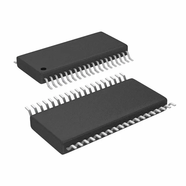
Housed in a 38-pin TSSOP (TFSOP) package with a 4.40 mm body width, surface-mount only.