What this LVDS buffer/multiplexer does on the board
The Texas Instruments SN65LVDS108DBTR is a 1:8 LVDS buffer and multiplexer that takes one differential LVDS input and fans it out to eight LVDS outputs. It is designed for clock and data distribution in high-speed serial backplanes, video links, and telecom line cards where signal integrity over multiple loads matters. The part accepts LVDS inputs and delivers LVDS outputs, maintaining the differential swing through the fanout tree. Rated for 400 Mbps per channel, the SN65LVDS108DBTR handles common serial protocols like LVDS video, gigabit Ethernet SERDES links, and high-speed ADC/DAC clock distribution without retiming. The 2.8 ns propagation delay is the pin-to-pin latency through the buffer — budget it in your timing closure for source-synchronous interfaces.
The 400 Mbps per-channel maximum covers most LVDS clock fanout and moderate-speed serial data distribution. For a 100 MHz clock, that's four times the fundamental — the buffer passes the third harmonic cleanly, keeping edge rates sharp. If your link runs at 1 Gbps or above per lane, this part is not the right fit; look at a redriver or retimer instead. The 5 pF input capacitance is low enough to not load the source driver excessively when the trace stub is short.
Package and layout realities
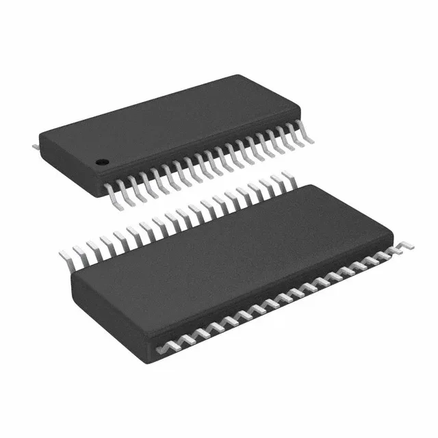
The 38-TSSOP footprint is shared with other TI LVDS fanout parts — check the base product number 65LVDS108 for pin-compatible siblings if you need a different fanout ratio.
This is a standard TI catalog part with broad distribution coverage.