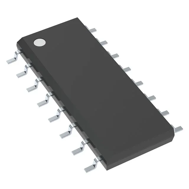
Texas Instruments SN65LVDS105DR — Interface & Transceivers

SN65LVDS105DR LVDS Buffer/Multiplexer, 400 Mbps, 16-SOIC

MPNSN65LVDS105DR
Active

Texas Instruments SN65LVDS105DR, LVDS Buffer/Multiplexer, LVTTL input, LVDS output, 1 x 1:4, 400Mbps data rate, 2.2ns delay, 3V–3.6V supply, -40°C to 85°C, 16-SOIC package.

$2.5173Ref. price · indicative, final on quote
Independent supplier — new & surplus stockAuthenticity-screened · ESD-safe packingListing updated Aug 2026

Specifications

SN65LVDS105DR specifications
ParameterValue
TypeBuffer, Multiplexer
MountingSurface Mount
Supply voltage3V ~ 3.6V
Current - supply23mA
Operating temperature-40°C ~ 85°C
InputLVTTL
OutputLVDS
PackageTape & Reel (TR)
Delay time2.2ns
Case16-SOIC (0.154\", 3.90mm Width)
Data rate400Mbps
Channels1 x 1:4
Capacitance - input3 pF

Product details

At 400 Mbps the SN65LVDS105DR can serialize a 40 MHz parallel bus into a single LVDS pair, or distribute a 200 MHz clock with sub-3 ns edge-to-edge skew across four outputs. The 2.2 ns propagation delay is the time from input crossing to output valid; in a clock tree this adds to the overall skew budget, so if you are fanning out a 100 MHz clock to multiple receivers, account for the delay mismatch between this buffer and any other devices in the path. The 3 pF input capacitance is light enough that a single LVTTL source can drive it without extra buffering.

Supply rails and signal levels

The LVTTL input threshold is compatible with 3.3 V logic families; the LVDS output delivers a differential swing of roughly 350 mV into a 100 Ω termination, standard for LVDS receivers. No external bias resistors needed on the output side — the driver handles the common-mode voltage internally.

Frequently asked questions

What is the data rate of SN65LVDS105DR?

Rated for 400 Mbps maximum, which corresponds to a 200 MHz clock frequency if used as a clock buffer. The 2.2 ns propagation delay and 3 pF input capacitance help maintain signal integrity at that speed.