400 Mbps LVDS fanout with LVTTL input
The 400 Mbps maximum data rate supports common serial interfaces like LVDS display links and high-speed backplane clock distribution. The 2.2 ns propagation delay leaves a clean timing budget for the receiving end — at 400 Mbps the bit period is 2.5 ns, so the delay consumes less than one unit interval, keeping the signal-integrity margin intact.
Runs from a single 3V to 3.6V supply, which means it drops straight onto a 3.3V rail without a separate regulator. The 23 mA supply current is the total for all four outputs driving — budget that into the 3.3V rail load. The 3 pF input capacitance on the LVTTL side is light enough that the driving FPGA or ASIC sees a minimal load, preserving the signal edge at 400 Mbps.
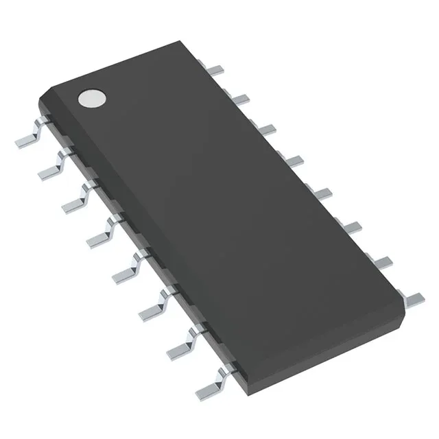
The supplier device package is 16-SOIC, surface-mount only. No exposed thermal pad, so the dissipation path is through the package leads and the board copper. At 23 mA and 3.6 V max, the internal dissipation is under 83 mW, well within the package's capability without special thermal management.
For BOM lines that need a second source, the SN65LVDS105DR is the tape-and-reel variant of the same die; the two are electrically identical, differing only in the shipping medium.