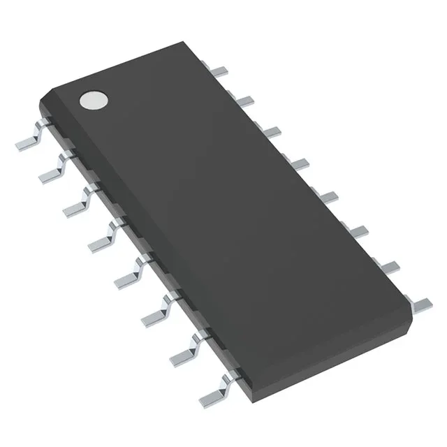
What this LVDS buffer/multiplexer does
The Texas Instruments SN65LVDS104DRG4 is a 1:4 LVDS buffer and multiplexer that takes one differential LVDS input and fans it out to four LVDS outputs.
The 400 Mbps data rate is the maximum serial bit rate each output channel can sustain. In practice, that gives you headroom for 100–200 Mbps LVDS links with plenty of margin on jitter and eye opening. The 3.1 ns delay is the propagation time from input to any output; when you are distributing a clock to multiple receivers, that delay adds to the overall skew budget. If your system requires matched delays across multiple fan-out paths, this part's single-channel architecture keeps the skew between outputs low — the datasheet typically specifies output-to-output skew well under 1 ns.
Where it fits: industrial and telecom backplanes
With its industrial temperature range and LVDS signalling, the SN65LVDS104DRG4 is a natural fit for distributing clock or data in factory automation controllers, motor drive feedback links, and outdoor telecom base station backplanes. The 3 pF input capacitance keeps the load on the driving source light, which matters when the source is another LVDS buffer or an FPGA with limited drive strength. The 16-SOIC package is a common footprint that fits standard PCB layout rules without fine-pitch routing.
The DRG4 suffix indicates a tape-and-reel shipping format, which is the standard for automated assembly lines.