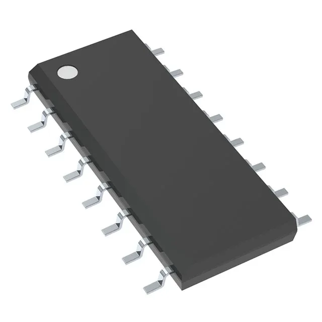
The Texas Instruments SN65LVDS104DR is a 1:4 LVDS buffer and multiplexer that takes one differential LVDS input and distributes it to four LVDS outputs. It is designed for clock and data distribution in high-speed digital systems where signal integrity over backplanes, cables, or PCB traces matters. Each output channel handles data rates up to 400 Mbps with a propagation delay of 3.1 ns, making it suitable for distributing serial links, clock signals, or parallel LVDS busses in telecom infrastructure, industrial automation, and test equipment.
400 Mbps per channel and 3.1 ns delay — the timing budget
The 400 Mbps data rate per output is the headline performance spec. In a clock distribution application, the 3.1 ns propagation delay means the output edges arrive about three nanoseconds after the input edge. For matched-length routing, you budget that delay into the overall skew calculation. The 3 pF input capacitance is low enough that a single LVDS source can drive the SN65LVDS104DR without extra buffering, even over a few inches of board trace.
16-SOIC package — board-level fit
The narrow SOIC footprint is common on mixed-signal boards where LVDS fanout sits near the connector or backplane interface. No exposed thermal pad — the 23 mA supply current is low enough that the package dissipates without extra copper.