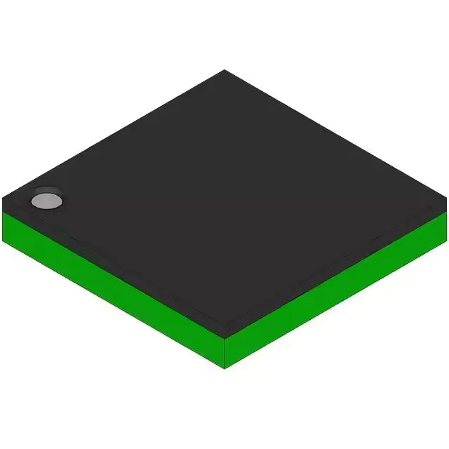
Boundary-scan test controller for JTAG-based board debug
The SCANSTA101SM from Texas Instruments is a microprocessor-circuit test-access controller that implements the IEEE 1149.1 (JTAG) interface — the standard protocol for board-level interconnect testing, in-system programming, and boundary-scan debug on dense digital assemblies.
49-ball BGA — rework and board-fit notes
Housed in a 49-LFBGA (7x7 mm) package, the SCANSTA101SM requires a standard surface-mount reflow profile for lead-free or tin-lead solder — but note the device itself is RoHS non-compliant, meaning the BGA balls carry a lead-bearing finish (typically Sn63Pb37 or high-Pb die-attach) and the assembly must be handled under the applicable RoHS exemption for legacy solder alloys used in test and measurement equipment. The 0.80 mm ball pitch on the 49-BGA is forgiving for a hand-assembly or rework station — a standard hot-air nozzle with a 10x10 mm aperture and a stencil thickness of 0.12 mm to 0.15 mm is adequate for prototyping or low-volume test-fixture builds.
JTAG interface and test-equipment deployment
The IEEE 1149.1 interface is the same JTAG port used by most FPGA, CPLD, and processor debug tools — the SCANSTA101SM acts as a bus master or access port controller in a boundary-scan chain, allowing a host controller to shift test vectors through the scan path of the board under test. This makes it a natural fit for automated test equipment (ATE), in-circuit test (ICT) fixtures, and diagnostic pods where the goal is to isolate opens, shorts, or stuck-at faults on dense BGA-based assemblies without physical probe access.