Fixed 3.3V output with ±0.2% initial accuracy
This is the accuracy you get at 25 °C without any external trimming — the reference sets the absolute voltage floor for your ADC, DAC, or sensor excitation circuit. The series topology means the output is regulated from the input rail, drawing a quiescent supply current of 135 µA typical.
For a 3.3 V output, that drift translates to roughly 66 µV per degree Celsius — a figure that determines whether your 12-bit or 16-bit measurement system holds its last few bits across the thermal envelope of a motor drive or outdoor telecom enclosure. Noise performance is specified as 43 µVp-p over the 0.1 Hz to 10 Hz band and 63 µVrms over 10 Hz to 10 kHz. The low-frequency flicker noise floor is the limiting factor for precision weigh-scale or strain-gauge front ends; the wider-band noise matters for ADC reference inputs where the converter samples at rates above the 1/f corner.
SOT-23-3 footprint and supply range
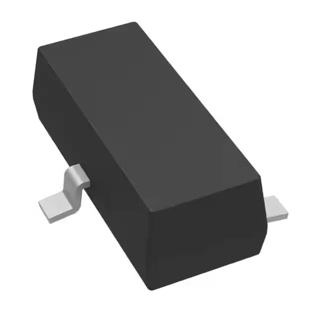
Housed in a 3-pin SOT-23-3 package (also described as TO-236-3 / SC-59), the device occupies minimal PCB area and suits standard surface-mount reflow assembly. The input voltage range is 3.35 V to 5.5 V, providing 50 mV of headroom above the 3.3 V output at the minimum — enough margin for a clean LDO or a 3.6 V lithium cell. The output is rated for 10 mA continuous current. That is sufficient to bias a single ADC reference input or a small sensor bridge; for multiple loads or higher drive, a buffer stage is needed.
The base part number is REF3133, and this specific suffix (AIDBZTG4) denotes the SOT-23-3 package with the extended temperature range.