1.8 GHz bandwidth, 1150 V/µs slew — what these mean on the bench
The OPA859IDSGR is a single-channel general-purpose operational amplifier from Texas Instruments, delivering a 1.8 GHz -3 dB bandwidth and a 900 MHz gain-bandwidth product. These figures mean it can amplify signals up to nearly 2 GHz before the gain drops by 3 dB — suitable for RF intermediate stages, high-speed ADC drivers, or wideband transimpedance amplifiers where preserving signal amplitude across frequency matters. Its 1150 V/µs slew rate ensures the output can track fast input transitions without slew-rate limiting, which would otherwise introduce nonlinear distortion on pulse edges or high-frequency sine waves. For a 1 V peak-to-peak output at 1.8 GHz, the required slew rate is roughly 11.3 V/µs — this part has over 100× margin, so slew-induced distortion is not a concern across the full bandwidth.
Package and thermal: 8-WSON with exposed pad
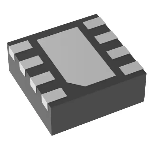
Housed in an 8-WFDFN exposed-pad package (supplier device package 8-WSON, 2 mm × 2 mm), the OPA859IDSGR is a surface-mount part with a thermal pad underneath. The exposed pad must be soldered to a PCB ground plane with thermal vias to achieve the datasheet thermal resistance — without this, the junction temperature rises above the -40°C to 125°C operating range under high output current or ambient heat. The 105 mA output current per channel means the part can drive 50-ohm loads to about 5.25 V swing — useful for driving transmission lines or high-speed ADC inputs directly. The 20.5 mA supply current is moderate for this speed class; the 3.3 V to 5.25 V supply span lets it run from a single 3.3 V or 5 V rail common in mixed-signal systems.
Active lifecycle and sourcing posture
The automotive-grade sibling OPA859QDSGRQ1 shares the same bandwidth and slew rate but adds AEC-Q100 qualification for -40°C to 125°C operation. If the end application requires automotive PPAP or reliability screening, the Q-grade variant is the drop-in replacement — same package, same pinout, same electrical performance.