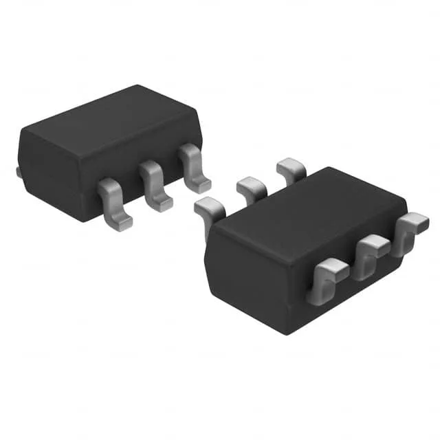
Package and board integration
The OPA838IDBVT comes in a 6-pin SOT-23-6 package (supplier device package SOT-23-6), a 2.9 mm × 1.6 mm footprint that fits tight channel spacing on multi-layer boards. Surface-mount assembly with standard reflow profiles — the small body limits the thermal pad area, so the junction-to-ambient thermal resistance is higher than larger packages; keep the copper pour under the device continuous to the ground plane for heat sinking. Supply span runs from 2.7 V minimum to 5.4 V maximum — the part works on a single 3.3 V or 5 V rail, or split supplies like ±2.5 V. The rail-to-rail output stage swings within 50 mV of each rail at light load, preserving dynamic range in low-voltage signal chains.
Speed and bandwidth trade-offs
300 MHz gain-bandwidth product (GBW) sets the small-signal closed-loop bandwidth: at a noise gain of 10, the -3 dB point lands near 30 MHz. The 350 V/µs slew rate defines the large-signal full-power bandwidth — a 2 Vpp output swing slews at 350 V/µs, supporting frequencies up to roughly 28 MHz before slew-rate limiting sets in. Voltage feedback architecture with a 1.5 µA input bias current — the bipolar input stage delivers the speed but draws bias current that flows through the source impedance. For a 1 kΩ source, the bias current creates a 1.5 mV DC error; for a 10 kΩ source it becomes 15 mV, which may need offset nulling or a FET-input alternative. Input offset voltage is 15 µV typical — good DC precision for a wideband amplifier, letting it serve in DC-coupled photodiode receivers or high-speed data acquisition front-ends without external trimming.
Power budget and thermal envelope
Quiescent supply current is 960 µA per channel — low enough to run continuously from a 3.3 V rail without a heat sink, even in multi-channel arrays. At 5 V supply, the static power dissipation is 4.8 mW; the SOT-23-6 package handles this with a junction temperature rise of about 15°C above ambient in still air. Operating temperature range spans -40°C to 125°C — industrial grade that covers outdoor base stations, engine-bay sensors, and factory-floor instrumentation. The 125°C upper limit means the part can sit next to a hot processor or power stage without derating.
Lifecycle and compliance
ROHS3 compliant, with no exemptions that would restrict EU or California market access.