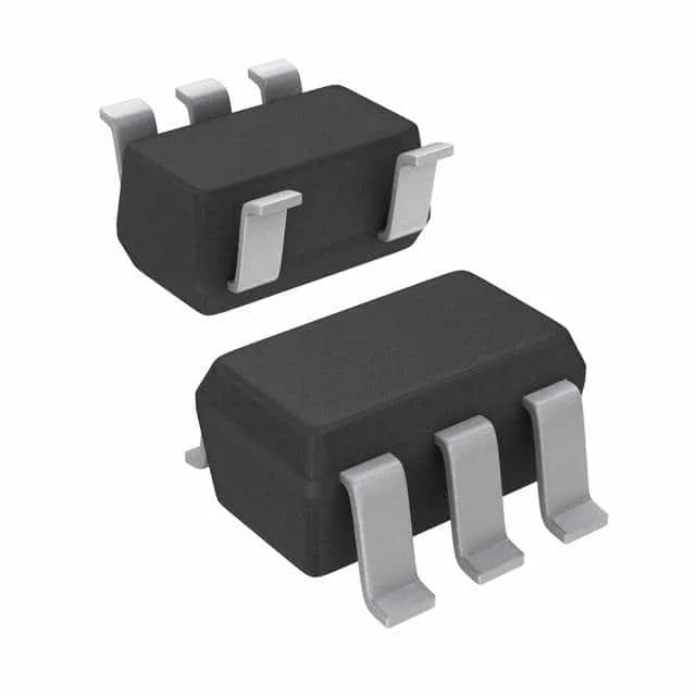
Texas Instruments OPA202IDBVR — Memory (DRAM / SRAM / Flash / EEPROM)

Texas Instruments OPA202IDBVR Op-Amp, 1 MHz, SOT-23-5

MPNOPA202IDBVR
End of Life

Texas Instruments OPA202IDBVR general-purpose operational amplifier, 1 MHz gain-bandwidth, 0.35 V/µs slew rate, 20 µV input offset, single circuit, SOT-23-5 package, Tape & Reel.

$1.35Ref. price · indicative, final on quote
PackagingSC-74A, SOT-753
RoHSROHS3 Compliant
Independent supplier — new & surplus stockAuthenticity-screened · ESD-safe packingListing updated Aug 2026

Specifications

OPA202IDBVR specifications
ParameterValue
Output typePush-Pull
MountingSurface Mount
Amplifier typeGeneral Purpose
Voltage - input offset20 µV
Voltage - supply span4.5 V
Current - supply580µA
Current - input bias250 pA
Current - output (Channel)35 mA
Operating temperature-40°C ~ 125°C
Gain bandwidth product1 MHz
PackageTape & Reel (TR); Cut Tape (CT)
Slew rate0.35V/µs
CaseSC-74A, SOT-753
Number of circuits1

Product details

1 MHz gain-bandwidth, 20 µV offset — precision DC performance in a compact SOT-23-5

The OPA202IDBVR is a single-channel general-purpose operational amplifier from Texas Instruments, offering a gain-bandwidth product of 1 MHz and a slew rate of 0.35 V/µs. With a maximum input offset voltage of 20 µV and input bias current of 250 pA, this op-amp is suited for precision DC signal conditioning in sensor interfaces, data acquisition, and control loops where external nulling is undesirable. The supply voltage range spans 4.5 V to 36 V, supporting both single-supply (e.g., 5 V or 24 V industrial rails) and split-supply configurations (±2.25 V to ±18 V).

Industrial temperature range and active production status

The OPA202IDBVR is an active-production device rated for the -40°C to 125°C industrial temperature range, making it suitable for factory-floor and outdoor equipment where ambient temperatures vary widely. The part is ROHS3 compliant and supplied in a standard SOT-23-5 package, which is a common footprint for compact PCB layouts in motor drives, PLC analog input modules, and temperature transmitters.

580 µA supply current and 35 mA output drive — power budget and load considerations

Quiescent current is 580 µA per amplifier, which keeps the thermal contribution low in multi-channel designs and extends battery life in portable instrumentation. The output stage can source or sink 35 mA, enough to drive the analog input of a typical SAR ADC, a small relay coil, or a 4-20 mA transmitter loop directly without a separate buffer.

Frequently asked questions

Is OPA202IDBVR suitable for single-supply applications?

Yes, the 4.5 V minimum supply voltage allows operation from a single 5 V rail. However, the output is not rail-to-rail — the push-pull stage will swing within about 1 V of each rail under moderate load. For a 5 V supply, expect a usable output swing of roughly 1 V to 4 V into a 10 kΩ load.

What is the closest functional alternative to OPA202IDBVR?

The TLV9351IDCKR is a pin-compatible alternative with a wider 3.5 MHz bandwidth and 20 V/µs slew rate, but it draws 600 µA supply current and has a 350 µV input offset. The OPA202IDBVR offers lower offset (20 µV) at the cost of slower speed — choose based on whether precision DC accuracy or signal bandwidth matters more.