That clock rate is the ceiling for instruction throughput — single-cycle core operations at 16 MHz give you a 62.5 ns instruction cycle, enough for sensor polling loops, simple control logic, and low-rate data processing.
Memory sizing — 8 KB Flash, 256 B RAM
Program memory is 8 KB of Flash (8K x 8), organized for sector erase. The 256 x 8 RAM is the working data space — enough for a few dozen variables, a small buffer, and the stack. If your firmware fits under 6 KB and the data set stays under 200 bytes, you have headroom. Beyond that, the next density step in the G2xx family doubles both Flash and RAM, which is the upgrade path if this part feels tight.
The MSP430 architecture is known for low active and standby current, though the exact numbers depend on clock configuration and peripheral use.
I/O and peripherals — 10 pins, I²C/SPI, 8-channel 10-bit ADC
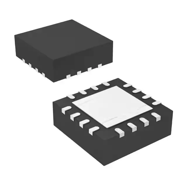
Ten I/O pins are available on the 16-QFN package. The DMA controller can move data between peripherals and memory without CPU intervention, which helps keep the core asleep longer in low-power applications.
Package and footprint — 16-QFN with exposed pad
The 4x4 mm footprint is compact but the pad pitch is fine — verify the solder-paste stencil aperture against the land pattern recommended in the datasheet.
Suitable for outdoor telecom enclosures, factory-floor sensors, automotive cabin (non-engine-bay) modules, and battery-powered IoT nodes that see seasonal temperature swings.