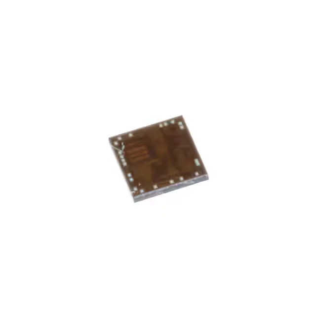
Bare-die MSP430 for embedded and hybrid builds
The die form factor eliminates the package overhead and saves board area, but it also means the part is not socketed or rework-friendly in the usual sense; assembly requires die-attach and wire-bonding capability.
Memory budget and peripheral set — what fits in 2 KB
With 2 KB Flash and 256 bytes of RAM, the firmware must be lean. The MSP430G2252TDA2 includes a 10-bit ADC with 8 multiplexed channels, a USI module supporting I²C and SPI, a PWM timer, brown-out detect, and a DMA controller — enough to handle a few analog sensors, a serial link to a host, and a control loop without external glue logic. The 16 I/O pins provide adequate headroom for a small keypad, LED indicators, or a parallel LCD interface. Designs that need more than 2 KB of code should look at the 4 KB or 8 KB Flash variants in the same die family (MSP430G2xx series), though the pin-compatibility and die footprint may differ.
Die handling and assembly considerations
There is no plastic or ceramic package — the silicon is the component. This changes the procurement and assembly process: the die requires a clean-room environment, die-attach epoxy or solder preform, and wire bonding to the substrate or PCB. Moisture sensitivity is inherent to the raw silicon; storage in a dry, inert atmosphere is recommended until assembly. For a packaged equivalent, the MSP430G2252 (without the TDA2 suffix) comes in a standard TSSOP or QFN package and is a drop-in functional match, though the board footprint and assembly process are completely different.
For dual-sourcing resilience, the packaged MSP430G2252 (TSSOP-20 or QFN-20) is a functional equivalent, though the board-level assembly differs.