1 KB Flash — the firmware-fit gate
The MSP430G2153IN20 carries 1 KB of Flash program memory (1K x 8) and 256 bytes of RAM (256 x 8). That is a tight memory envelope — suitable for a single-purpose control loop, a sensor node state machine, or a simple LIN-bus translator, but not for a multitasking firmware stack or OTA update staging. The buyer should confirm the compiled image fits within 1 KB before committing the BOM line; a 2 KB or 4 KB sibling in the same MSP430G2xx series costs a few cents more and avoids a last-minute code-size surprise.
The internal DCO and the on-chip brown-out detect/report block (BOR) keep the core alive across that range without an external supervisor. For a battery-powered sensor node or a field-transceiver module, this part can run directly from the battery rail through most of its discharge curve.
16 MHz core — timing margin with the internal oscillator
The CPU16 core runs at 16 MHz, driven by an internal oscillator that eliminates the external crystal and its two load capacitors. At 16 MHz the flash needs zero wait states — the core fetches instructions in a single cycle, so there is no timing-closure surprise when you ramp the PLL. The IrDA, LINbus, and SPI peripherals can run at full clock speed without bit-rate division, which simplifies the baud-rate generator configuration.
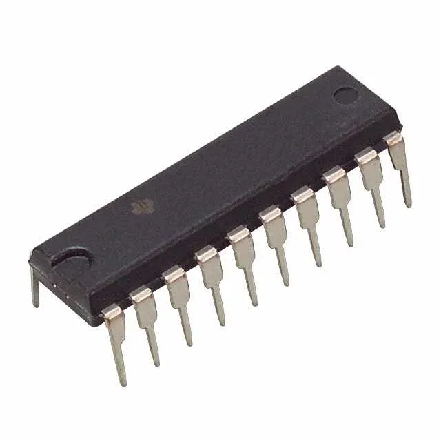
The 20-pin DIP package (20-DIP, 0.300" body width) is through-hole — it survives rework cycles and manual assembly better than a QFP, and the plastic DIP handles the thermal cycling of an industrial environment without cracking the die attach.
New designs can proceed without a near-term end-of-life risk, and the through-hole DIP package means the part is still stocked by broadline distributors for legacy product support.