128 B RAM — sizing the firmware budget
The 128 x 8 RAM is the real constraint on this part. It limits the call stack depth and the size of runtime buffers, so firmware needs to be lean — think single-variable control loops, not multi-frame packet handling. The 1 KB Flash can hold a modest interrupt-driven I²C or SPI slave routine plus a state machine, but leave no room for OTA staging or a full bootloader. For designs that need more headroom, the MSP430G2xx family offers pin-compatible parts with up to 8 KB Flash and 512 B RAM, but the 128 B RAM here keeps the die small and the active current low.
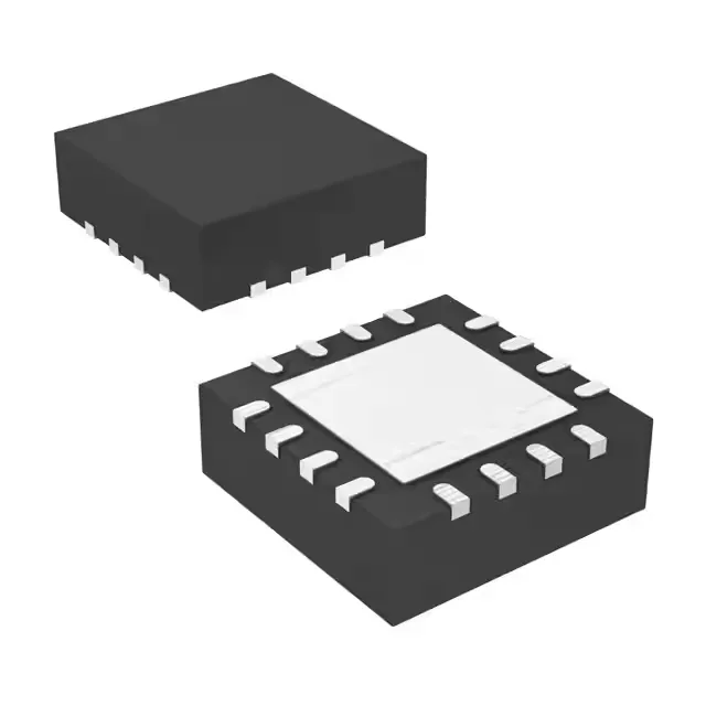
16-VQFN with exposed pad — rework considerations
The part comes in a 16-VQFN exposed-pad package (4x4 mm body). The QFN is reworkable with hot air if you pre-bake the board (MSL level not stated, but assume MSL 3 as typical for this package class). The 16-QFN footprint is shared across the MSP430G2xx family, so a board designed for this part can also accept higher-memory siblings without layout changes.