16 MHz, 1 KB Flash, 128 B RAM — the memory-constrained ultra-low-power MCU
1 KB Flash and 128 B RAM — what the memory budget means
With 1 KB of Flash and 128 bytes of RAM, this part is not for complex protocol stacks or data logging. The Flash holds the firmware image; the RAM handles a small stack, a few global variables, and an interrupt context. A typical application reads one or two analog signals through an external ADC (this part has no on-chip ADC per the peripheral list — brown-out detect, POR, PWM, and WDT are the on-chip blocks), drives a PWM output for a small motor or LED, and communicates over a bit-banged UART or I²C on the 10 available I/O pins. Firmware updates over the air are impractical — the Flash is too small for a bootloader plus application image. The design assumes the firmware is locked at manufacture.
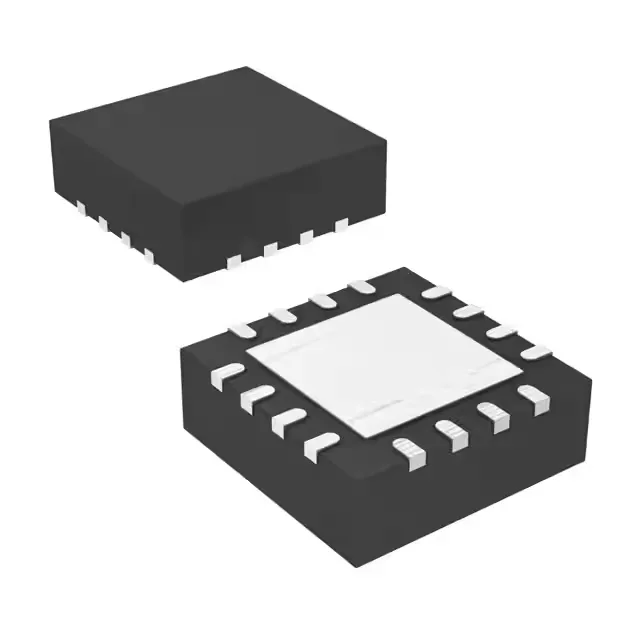
Housed in a 16-VQFN exposed-pad package (4x4 mm body, supplier device package 16-QFN), it is a surface-mount part for reflow assembly.