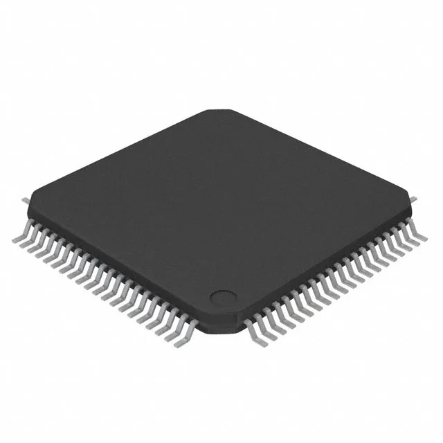
FRAM-based 16-bit MCU for low-power edge control
Its program memory is 256 KB of FRAM — a non-volatile memory that writes at bus speed with essentially unlimited endurance, unlike Flash.
FRAM: what it changes for the firmware and BOM
FRAM eliminates the erase-before-write cycle that Flash requires. That means the firmware can treat the 256 KB memory as uniform storage — code, config parameters, and data logging all share the same space without a wear-leveling layer. Write endurance is effectively unlimited for field updates, and writes happen at the 16 MHz bus speed with no wait states. For a design that logs sensor data or stores calibration constants, this removes the EEPROM or serial FRAM chip from the BOM.
The 16 MHz clock is the ceiling for the CPUXV2 pipeline. This is not a number-crunching core — it is sized for control-loop tasks, sensor polling, and protocol handling at moderate rates. The trade-off is power: the MSP430 family is architected for sub-milliamp active draw and microamp sleep currents, so the 16 MHz part fits battery-powered or energy-harvesting nodes where a 100 MHz Cortex-M would overshoot the power budget.
Industrial temperature grade and deployment context
For indoor commercial equipment the temperature margin is generous.
Package and I/O — board-fit notes
The 80-LQFP (12x12 mm) with 68 GPIOs gives the layout engineer a dense but routable footprint. The 0.4 mm pitch is fine for two-layer boards with careful trace spacing; four-layer designs have no trouble.
It is ROHS3 compliant.