256 KB FRAM — the reason to pick this over a Flash MCU
FRAM writes at bus speed with essentially no endurance limit — 10^15 cycles versus Flash's 10^4–10^5 — and consumes microamps in standby while retaining data. That makes this part a fit for data-logging, metering, and battery-operated edge nodes where frequent nonvolatile writes or instant-on wake from deep sleep matters. The 20-channel 12-bit ADC, hardware multiplier, and DMA engine handle sensor aggregation without loading the core.
Supply, temperature, and the 87-ball BGA footprint
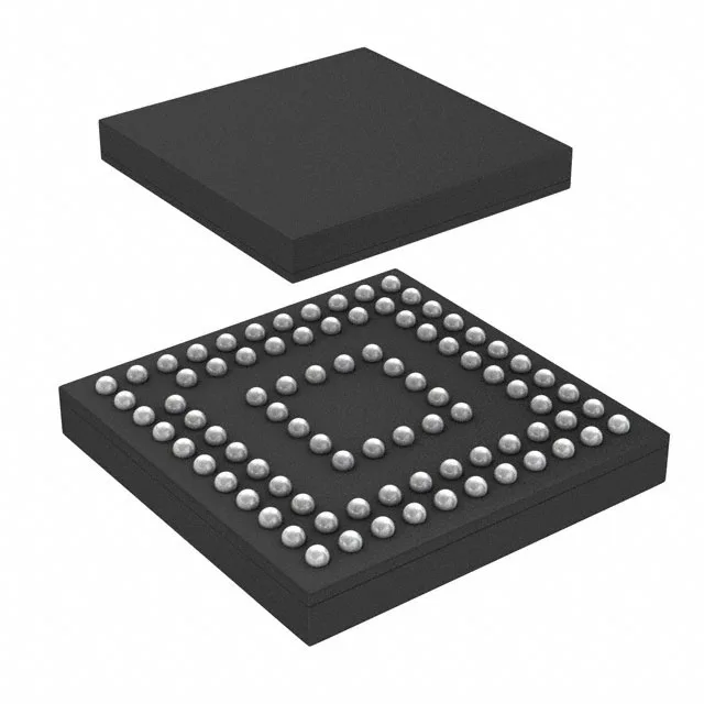
Package is an 87-ball NFBGA measuring 6 mm × 6 mm — fine-pitch BGA with 0.5 mm or 0.65 mm ball pitch depending on the specific die revision. That footprint needs a controlled-impedance fanout pattern and a stencil matched to the ball diameter; don't assume a generic BGA escape works without checking the TI recommended land pattern.
Peripherals and debug reality
68 GPIOs, I²C, SPI, UART/USART, plus IrDA for optical links. Brown-out detect, POR, and watchdog are on-chip — no external supervisor needed for basic safety. The CPUXV2 core has a single-cycle 32-bit hardware multiplier and a 3-stage pipeline; at 16 MHz it delivers about 16 MIPS. Debug is via the standard Spy-Bi-Wire (SBW) two-pin JTAG interface. MSP430Flasher works with this device as long as the toolchain version supports the FR59xx family — check the release notes for the specific FRAM controller revision.
The base product number MSP430FR59941 covers a density and feature set that TI continues to support. For a dual-sourcing review, the MSP430FR5994 (without the trailing '1') is the same die in a different test-program variant — verify pin compatibility against the TI cross-reference before swapping.