What this MSP430FR5858IRHAR brings to the board
Its program memory is 48 KB of FRAM — non-volatile, fast-write, and rated for far more erase/write cycles than Flash, so you can treat it like a unified memory for code and data without worrying about wear leveling. The 2K x 8 RAM handles stack and scratchpad. On the analog side you get a 14-channel 12-bit ADC, enough for a multi-sensor input stage without external muxing.
FRAM vs Flash — why it matters for field updates
The 48 KB FRAM program memory is the headline feature. That means you can log data or update firmware in the field without an external EEPROM and without wear-leveling logic in software. For a product that ships once and gets OTA updates for years, this saves BOM cost and firmware complexity.
Package and footprint — what the rework tech sees
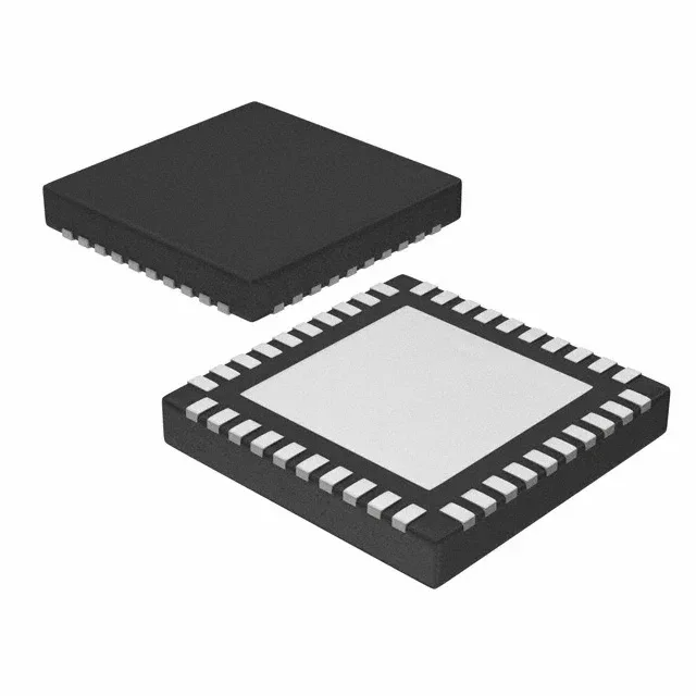
The MSP430FR5858IRHAR comes in a 40-VFQFN with an exposed thermal pad (40-VQFN 6x6 mm per the supplier device package).
That means standard lead times through distribution, no LTB math needed, and full manufacturer support for new designs.