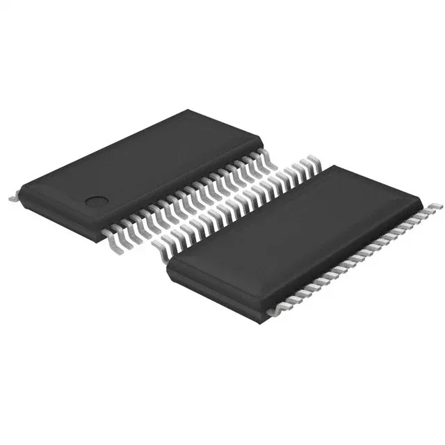
Texas Instruments MSP430FR5848IDA — Microcontrollers & Processors (MCU / MPU / DSP)

TI MSP430FR5848IDA 16-bit MCU, 48KB FRAM, 16MHz, 38-TSSOP

MPNMSP430FR5848IDA
Active

Texas Instruments MSP430™ FRAM series, MSP430FR5848IDA, 16-Bit Microcontroller, 16MHz, 48KB (48K x 8) FRAM, 2K x 8 RAM, 31 I/O, I²C/SPI/UART/IrDA, 38-TSSOP, -40°C to 85°C, 1.8V to 3.6V

$5.9400Ref. price · indicative, final on quote
Packaging38-TSSOP (0.240", 6.10mm Width)
RoHSROHS3 Compliant
SeriesMSP430™ FRAM
Independent supplier — new & surplus stockAuthenticity-screened · ESD-safe packingListing updated Aug 2026

Specifications

MSP430FR5848IDA specifications
ParameterValue
SeriesMSP430™ FRAM
MountingSurface Mount
Oscillator typeInternal
Program memory typeFRAM
Voltage - supply (Vcc (Vdd))1.8V ~ 3.6V
Operating temperature-40°C ~ 85°C (TA)
Speed16MHz
PackageTube
RAM size2K x 8
Core size16-Bit
PeripheralsBrown-out Detect/Reset, DMA, POR, PWM, WDT
ConnectivityI²C, IrDA, SCI, SPI, UART/USART
Number of i (O)31
Core processorMSP430 CPUXV2
Case38-TSSOP (0.240\", 6.10mm Width)
Data convertersA/D 12x12b
Program memory size48KB (48K x 8)

Product details

Active production — safe for new designs

The MSP430FR5848IDA: This means it remains a current-production choice for both prototype builds and volume manufacturing runs, with standard lead times through the distribution channel.

FRAM memory — unified program and data storage

This MSP430FR5848IDA integrates 48KB of FRAM as its program memory. The 2K x 8 SRAM complements the FRAM for stack and scratchpad use, while the unified memory map lets you treat FRAM as both code space and nonvolatile storage without separate banks.

The 16 MHz clock rate on the 16-bit RISC core delivers roughly 16 MIPS. That is sufficient for sensor fusion loops running at a few kilohertz, real-time PID control, UART/I²C protocol handling, and low-speed data logging.

The 1.8V to 3.6V supply range lets it run directly from two AA cells (down to 1.8V with the brownout detect monitoring the rail) or from a standard 3.3V regulated supply.

38-pin TSSOP — footprint and routing

Housed in a 38-TSSOP package (0.240" body width, 6.10mm), the MSP430FR5848IDA offers 31 general-purpose I/O pins. That is a high GPIO count for a 38-pin package, useful for parallel interfaces to character LCDs, keypad matrices, or multiple sensor interrupts. The TSSOP body is narrow enough for two-layer board routing in most designs, and the 0.65mm pitch is hand-solderable with care. Surface-mount assembly is standard; no exposed thermal pad to stitch.

On-chip peripherals include a 12-channel 12-bit ADC, brownout reset, power-on reset, DMA controller, and multiple timer/PWM channels. The DMA can move ADC results to FRAM without CPU intervention, which keeps the core asleep longer in duty-cycled applications.

Frequently asked questions

What is the difference between MSP430FR5848IDA and MSP430FR5849IDA?

The MSP430FR5849IDA is a higher-density sibling in the same FRAM family, offering 64KB of FRAM versus the 48KB on the MSP430FR5848IDA. Both share the same 38-TSSOP package, 16 MHz CPUXV2 core, 2K x 8 RAM, and peripheral set — the difference is the program memory size for firmware that exceeds 48KB.

How to program MSP430FR5848IDA?

Programming uses TI's standard Spy-Bi-Wire (SBW) or JTAG interface through the MSP430 debug probes (e.g., MSP-FET, MSP-EXP430FR5739 LaunchPad). The FRAM can be written at full speed with no erase cycle, so firmware updates complete faster than with Flash-based MCUs. TI's Code Composer Studio and IAR Embedded Workbench both support the MSP430 CPUXV2 architecture.