FRAM-based 16-bit MCU for low-power sensing and control
FRAM combines non-volatile storage with write speeds approaching SRAM and endurance far beyond flash—useful for data-logging applications where the MCU writes to memory on every sensor readout without wearing out sectors.
For BOM planning, this removes the urgency of finding a drop-in substitute or stocking up on lifetime buys. The part is ROHS3 compliant.
The 24 MHz clock rate is the CPUXV2's maximum operating frequency. At this speed, FRAM program memory requires no wait states, so instruction fetch cycles are deterministic—important for real-time control loops where jitter in execution time can upset timing margins. The 8 KB FRAM size (8K x 8) is enough for mid-complexity firmware: sensor calibration tables, communication protocol stacks, and state machines. The 1K x 8 SRAM covers stack, heap, and small data buffers. If your application needs more RAM for large packet buffers or extensive lookup tables, consider the higher-density siblings in the MSP430FR57xx family. The 17 I/O pins, combined with the internal oscillator, allow a minimal two-wire programming/debug interface (SBW) plus a handful of sensor or actuator lines—enough for a compact sensor node or a simple human-machine interface.
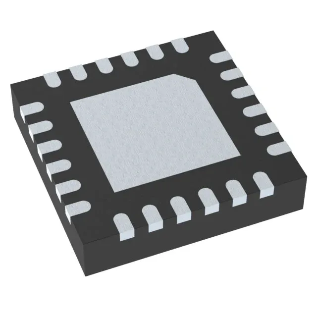
Package and footprint: 24-VQFN with exposed pad
Housed in a 24-VFQFN exposed-pad package (4x4 mm body, supplier device package 24-VQFN), the MSP430FR5732IRGET is a surface-mount device. The pad also provides a low-inductance ground return for the digital switching currents, which helps keep EMI under control.