What makes this MCU different: FRAM instead of Flash
Its standout feature is 4 KB of FRAM program memory — a non-volatile memory that writes at near-SRAM speed, consumes far less active power than Flash, and supports over 10^15 write cycles.
24 MHz CPU speed — enough for sensor fusion and control loops
24 MHz is modest compared to Cortex-M parts, but the MSP430 architecture is designed for efficiency at low clock speeds. The CPUXV2 core executes most instructions in one or two cycles, so 24 MHz delivers around 12–16 MIPS — sufficient for real-time control loops, sensor polling at kHz rates, and communication protocol handling.
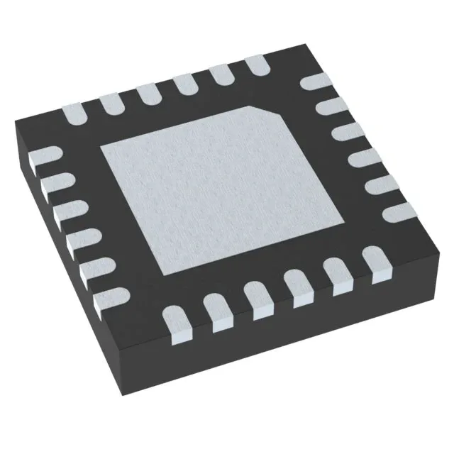
Package and footprint: 24-VQFN with exposed pad
The exposed pad must be connected to ground (or the appropriate supply plane) for proper thermal and electrical performance. The 17 I/O pins are all 5 V tolerant, simplifying level-shifting when interfacing with older logic families.
Peripherals and data converters: built-in ADC and serial interfaces
An 8-channel, 10-bit ADC is integrated, suitable for reading analog sensors like temperature, light, or potentiometers. The Brown-out Detect/Reset and POR circuits ensure reliable startup and operation during supply transients. The PWM timer supports motor control or LED dimming, and the watchdog timer (WDT) provides system-level fault recovery. Connectivity includes I²C, SPI, UART, LINbus, and IrDA — enough to talk to most common peripherals without external protocol chips.