8 MHz CPU with FRAM — the power budget decision
The MSP430FR5729IDA runs the 16-bit MSP430 CPUXV2 core at 8 MHz, a speed tier that keeps dynamic current under 200 µA/MHz in active mode while the FRAM program memory eliminates the write-cycle limits of flash — no erase-before-write penalty, no 10-year retention worry.
Peripheral set for sensor-fusion nodes
Fourteen 10-bit ADC channels capture analog inputs from temperature, pressure, or current-sense elements without an external multiplexer. The I²C, SPI, UART, and LINbus connectivity covers both local sensor buses and vehicle network interfaces — the LIN physical layer is integrated, so a LIN transceiver is the only external component needed for an automotive sub-node. Thirty GPIOs in the 38-TSSOP package leave enough headroom for a small keypad or a parallel LCD after allocating the serial peripherals.
Industrial temperature range and on-chip supervision
The integrated brown-out reset, power-on reset, and watchdog timer eliminate three external ICs from the BOM: the BOR holds the core in reset until the supply crosses the threshold, the POR ensures known startup state, and the WDT guards against firmware lockups without a separate supervisor.
Active production — sourcing posture
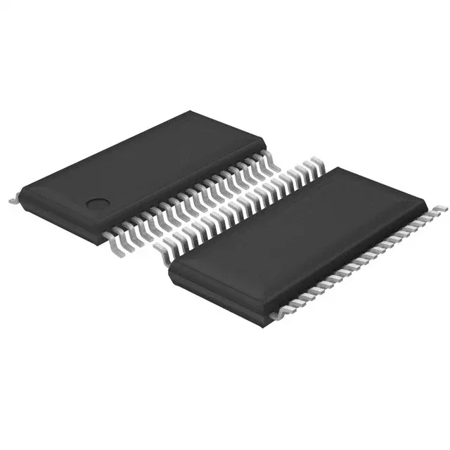
The base product number MSP430FR5729 covers the full family variant — the IDA suffix denotes the 38-TSSOP package and industrial temperature grade.
Package footprint notes for layout
The 38-TSSOP package has a 0.65 mm lead pitch and a 6.10 mm body width — the footprint fits on a two-layer board with 0.25 mm trace widths and 0.30 mm via drill. The supplier device package designation 38-TSSOP matches the standard JEDEC MO-153 profile; no exposed thermal pad, so the ground slug is not a requirement. Surface-mount assembly with standard reflow profile per IPC/JEDEC J-STD-020.