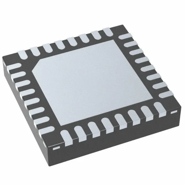
32 KB FRAM at 24 MHz — the unified-memory MCU for sensor and control loops
Its defining feature is 32 KB of FRAM (ferroelectric RAM) program memory — a non-volatile storage technology that combines the speed of SRAM with the persistence of Flash, and supports byte-level writes at near-zero power. This makes it a strong fit for applications that log data, update firmware over the air, or wake frequently from low-power modes, where Flash write cycles and erase overhead become a bottleneck.
FRAM vs Flash — what the memory type means for your firmware strategy
The MSP430FR2155TRSMT eliminates the EEPROM emulation overhead and the write-cycle budgeting that Flash-based MCUs require. For a design that stores sensor offsets or updates a lookup table in the field, this is the difference between a 100k-cycle endurance limit and effectively unlimited write endurance — the FRAM cell is rated for 10^15 read/write cycles. The trade-off is density: 32 KB is modest compared to Flash parts in the same price tier, so firmware size must be managed tightly.
Brown-out detect and POR are integrated, so the reset circuit on the board can be minimal.
The 8-channel 12-bit SAR ADC samples at rates sufficient for most sensor-fusion and feedback-control loops. An internal oscillator is available, but the device also supports an external crystal for applications requiring tighter timing accuracy. The 28 I/O pins in the 32-VQFN package leave room for a 16x2 LCD segment driver or a matrix keypad alongside the serial buses.
The part is ROHS3 compliant. For production planning, this means standard lead times through distribution and no forced redesign horizon. The base product number MSP430FR2155 covers the family; density variants share the same footprint, so a migration to a larger FRAM part is a BOM-line change without a board spin.