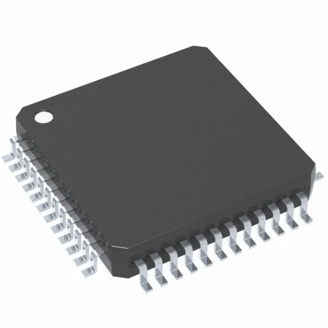
The 24 MHz clock, 4K x 8 SRAM, and integrated peripherals (12-bit ADC with 12 channels, I²C, SPI, UART, PWM, brown-out reset) target real-time control and sensor-fusion tasks in industrial and automotive-adjacent environments.
FRAM: the spec that changes the firmware strategy
FRAM writes at the full 24 MHz bus speed with no erase-before-write cycle. For firmware teams coming from Flash-based MSP430F parts, this means you can treat the 32 KB program space like RAM that holds its state through a power cycle — OTA staging, calibration tables, and data-logging buffers can share the same memory without wear-leveling logic. The 4K x 8 SRAM handles stack and fast variables; the FRAM handles persistent state with write endurance orders of magnitude beyond EEPROM.
Supply voltage and power rail design
No external level shifters are needed for the 44 GPIOs when interfacing with 3.3 V logic peripherals. The internal oscillator (no external crystal required for basic clocking) saves two pins and a PCB footprint, though the 24 MHz PLL still needs the flash wait-state configured correctly at power-up — a standard step in the MSP430 clock-tree initialization.
No exposed thermal pad — junction temperature is managed through the package body and airflow, so keep the ambient below 105°C and ensure adequate copper area on the inner layers for heat spreading.