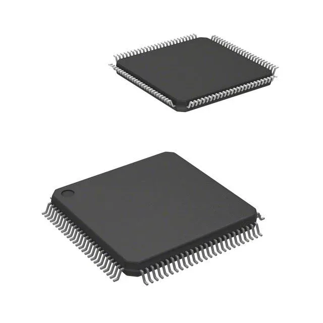
The 100-LQFP package (14x14 mm) provides 80 I/O lines, and the operating temperature range of -40°C to 85°C suits industrial and outdoor telecom enclosures.
Obsolete — sourcing reality for this BOM line
No official pin-compatible successor from TI has been published for this specific variant. If your design can tolerate a different peripheral set or memory density, a cross-reference search against the MSP430x4xx family may yield a drop-in footprint match — but that is a separate engineering validation, not a sourcing shortcut.
At 8 MHz, this MCU is not a high-throughput processor. It is sized for low-duty-cycle sensor polling, serial protocol handling, and display updates — not for real-time DSP or fast control loops. The 12-bit ADC and DAC operate within that clock budget; expect conversion rates in the tens of ksps range, adequate for temperature, pressure, or battery monitoring. The integrated LCD driver offloads display refresh from the CPU, so the 8 MHz ceiling does not limit a segment-count-heavy HMI. DMA moves data between ADC and RAM without core intervention, preserving throughput for the serial interfaces.
Mixed-signal integration — ADC and DAC on-chip
The 12-bit ADC with 12 multiplexed inputs and the dual 12-bit DAC eliminate external data converters in many instrumentation and closed-loop control designs. The ADC shares the analog supply pin with the rest of the MCU; keep the analog reference clean with a local decoupling cap near the AVcc pin.