What the 20 MHz core and memory mean for your BOM line
This is the mid-range density option in the MSP430F6xx family — enough headroom for a USB stack, a real-time control loop, and a modest data buffer, but not the 512 KB / 32 KB tier for heavy graphics or audio processing. The 20 MHz clock is the ceiling for the CPU and the peripheral bus; at that speed the flash needs zero wait states for most linear code, but tight loops or DMA transfers benefit from the internal prefetch buffer. If your application runs a USB device stack at full speed (12 Mbps) alongside a 12-bit ADC sampling at 200 ksps, the 20 MHz core has the margin to handle both without stalling the control loop.
Mixed-signal peripherals: ADC and DAC count
This part integrates a 16-channel, 12-bit successive-approximation ADC and two 12-bit DACs. For a sensor-fusion node reading multiple analog inputs (thermistors, current shunts, strain gauges) and outputting a control voltage or a setpoint, the ADC channel count and DAC resolution are the deciding specs. The 12-bit resolution is adequate for 0.1% measurement accuracy with proper reference and layout; if your design needs 16-bit or differential inputs, you would step up to the MSP430F6xx with the sigma-delta ADC option.
Package reality: 113-NFBGA (7x7)
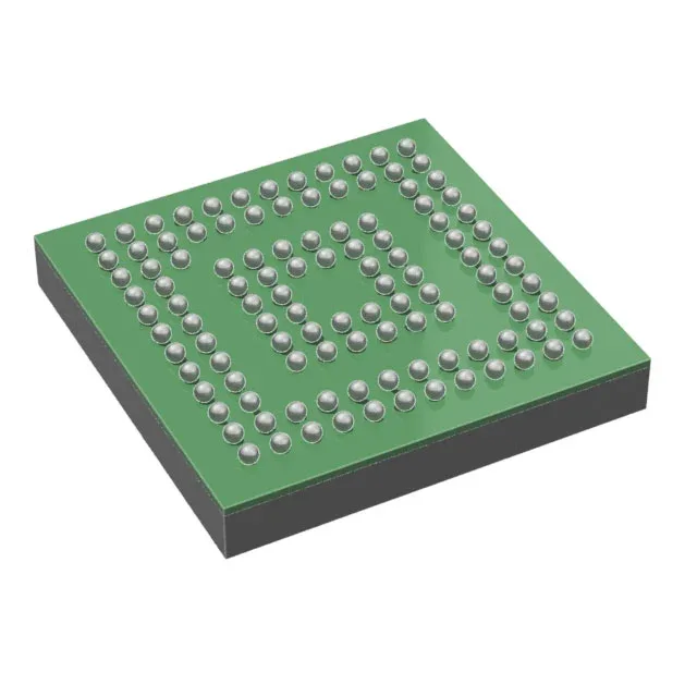
The MSP430F6638IZCAR comes in a 113-ball NFBGA package measuring 7 mm square. This is a fine-pitch BGA — not a hand-solderable part. The board requires a controlled-impedance stackup, microvias or via-in-pad for the inner balls, and a reflow profile with a peak temperature around 245 °C. The 74 I/O are distributed across the BGA ball map; the datasheet ball-out is essential for the PCB layout, especially the USB DP/DM differential pair and the analog supply pins.