What the 20 MHz core and 128 KB flash mean for a BOM line
The MSP430F6433IZQWR is a 16-bit MSP430 CPUXV2 core running at 20 MHz — the clock ceiling for this family, so the instruction cycle time is 50 ns. That 128 KB of on-chip flash (128K x 8) and 10 KB of SRAM (10K x 8) mean the part handles moderate-sized application code and a real-time data buffer without external memory. The 74 I/O lines, mapped to the 113-VFBGA package, give enough headroom for a parallel LCD bus, keypad matrix, and sensor interfaces on a single chip. The peripheral set includes a DMA controller, a hardware multiplier, an LCD driver, brown-out reset, POR, PWM, and a watchdog timer — all on-chip. Connectivity covers I2C, IrDA, LINbus, SCI, SPI, and UART/USART, so it can talk to serial sensors, a CAN transceiver via the LIN module, or a host controller over SPI without external protocol glue.
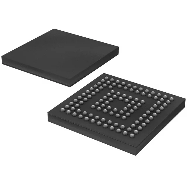
Package and board-fit — 113-BGA Microstar Junior
The 113-VFBGA package (Supplier Device Package: 113-BGA Microstar Junior, 7x7 mm) is a fine-pitch BGA — the ball pitch is 0.50 mm, so the PCB requires a 4-layer stack-up with microvias or via-in-pad for fan-out. The internal oscillator eliminates the external crystal for the main clock, saving two pins and a PCB footprint slot.
Texas Instruments has marked the MSP430F6433IZQWR as Obsolete. That means the manufacturer no longer produces it, and no official last-time-buy window remains open. If the design is still in development, a migration to a current MSP430F6xx variant in a similar BGA package should be evaluated — the peripheral set and core architecture are consistent across the family, but the pinout and memory map differ.