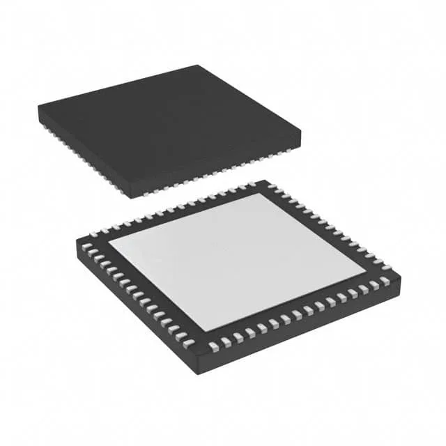
What this MSP430F5513IRGCR brings to a mixed-signal BOM
The 64-VFQFN (9x9 mm) package with exposed pad gives 47 general-purpose I/O lines. This is a part aimed at battery-powered or low-power instruments that need a USB link — data loggers, handheld medical meters, portable sensor hubs, and industrial control panels that talk to a host over USB or a serial bus.
The 25 MHz clock on the MSP430 CPUXV2 core is the practical limit for single-cycle instruction throughput on this 16-bit architecture. It is fast enough to handle a 100 kHz control loop with sensor read, PID math, and USB packet handling in the same frame, but it is not a DSP-class number — you are buying deterministic low-power execution, not MIPS bragging rights. The 25 MHz ceiling also sets the flash wait-state boundary; the CPUXV2 can run from Flash at 25 MHz with zero wait states, so no timing closure headache on the memory bus.
The 32 KB Flash is the firmware budget — enough for a USB stack, a command parser, and a moderate application state machine, but tight if you are trying to cram a GUI library or a full FAT filesystem. The 6 KB RAM (organized as 6K x 8) is split between general-purpose SRAM and the USB buffer. For designs that log data or buffer USB packets, watch the RAM allocation: the USB endpoint buffer takes a chunk out of the 6 KB, so the application heap and stack need careful sizing. This memory tier is a good fit for a single-function instrument that streams readings over USB, not a multitasking gateway.
USB plus serial — the connectivity mix that defines the application
That combination targets designs where a microcontroller talks to a PC or charger over USB while also managing a sensor array over I²C or SPI, or driving a LIN bus in an automotive-adjacent module. The LINbus and IrDA support are less common on competing 16-bit MCUs at this price tier, so if your BOM needs both USB and LIN, this part saves an external bridge chip.
At the low end, 1.8 V operation with the internal oscillator keeps the core alive during battery brownout without a separate boost converter.
Package and PCB layout notes for the 64-VQFN
The exposed paddle is the primary thermal path — without a 3x3 or 4x4 via matrix stitched to an inner ground plane, the junction temperature climbs under sustained USB activity at 85°C ambient. The 0.5 mm pitch on the perimeter pads is standard for QFN assembly; no exotic stencil aperture needed. The 47 I/O lines are all on the perimeter, so routing to a two-layer board is feasible if the ground plane is kept intact under the package.
That means it is still in normal production with no announced last-time-buy or end-of-life notice. The base product number MSP430F5513 covers the whole density and package family, so if the 64-VQFN package or the 32 KB Flash tier is the fit, the supply channel is stable through TI's distribution network.