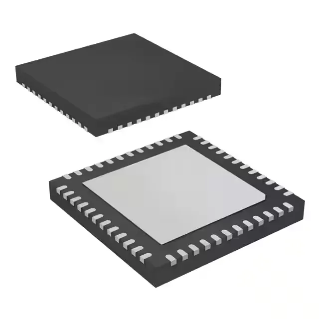
USB-enabled 16-bit MCU for mixed-signal control
The 25 MHz clock rate is enough to run a USB stack with packet handling while leaving MIPS for sensor polling or a control loop. The USB peripheral (full-speed, not high-speed) integrates the PHY and transceiver, so no external USB chip is needed — that saves board area and BOM cost. The 32 KB Flash and 6 KB RAM are sized for a typical USB CDC or HID class implementation plus application code; if your firmware needs a larger heap or OTA staging area, you will want to budget the RAM against the 6 KB ceiling.
Package and layout: 48-VQFN with exposed pad
The 31 I/O pins are all 5 V tolerant, which simplifies level interfacing with older logic families.
For dual-sourcing, the MSP430F5508 is a pin-compatible sibling with 48 KB Flash — verify the memory map difference against your firmware image size before substituting.