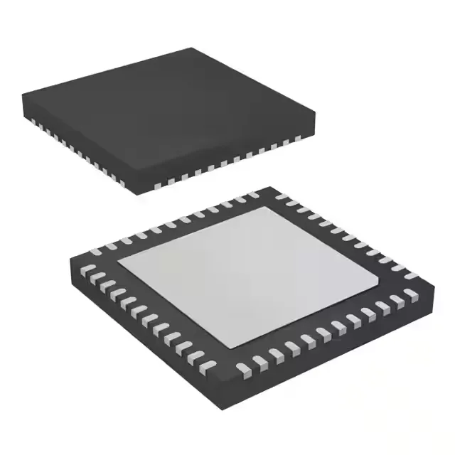
It carries 24KB of Flash program memory and 6K x 8 of RAM, enough for moderate-sized control firmware with a USB stack and sensor fusion.
Memory sizing: 24 KB Flash, 6 KB RAM
The 24KB Flash (24K x 8) and 6K x 8 RAM set the firmware budget. For a USB CDC or HID class implementation with a handful of ADC channels and a control loop, this is comfortable. If the application needs a full USB mass-storage stack with a FAT filesystem and a large lookup table, the RAM will be tight — budget the linker map early. The 6KB is SRAM, not cache; every byte is directly addressable by the CPUXV2.
Supply range and brown-out protection
Operates from 1.8V to 3.6V supply, so it can run from a single Li-ion cell or a 3.3V regulated rail. The integrated brown-out detect and POR circuits hold the core in reset until the supply is stable — no external supervisor needed for basic power-fail safety. The DMA and PWM peripherals keep running without CPU intervention once configured, which matters for time-critical output sequences.
For dual-sourcing resilience within the same family, the MSP430F550x series shares pin-compatible footprints across density options (24KB to 64KB Flash), so a firmware-only migration is possible without a board spin.