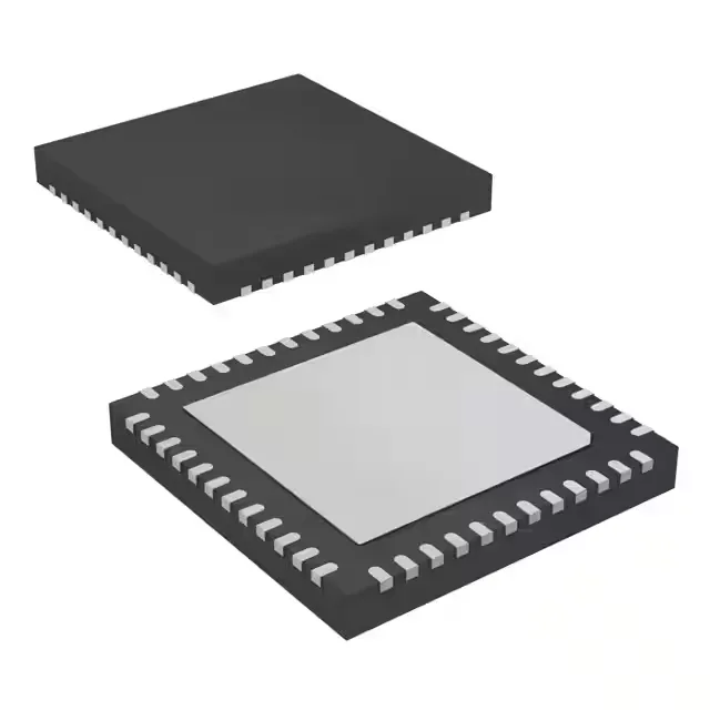
48-VQFN package and board integration
The MSP430F5503IRGZR ships in a 48-VFQFN with exposed pad, supplier device package 48-VQFN (7x7 mm). Surface-mount only. Decoupling capacitors should sit within 3 mm of each VCC/VSS pair to keep the supply impedance below 1 Ω at the 25 MHz core clock edge.
25 MHz CPUXV2 core with USB 2.0
The 16-bit MSP430 CPUXV2 core runs at 25 MHz, delivering roughly 25 MIPS from flash with zero-wait-state execution up to 8 MHz; beyond that, one wait state is inserted per access. The internal oscillator trims to ±1% accuracy over temperature, so a USB full-speed (12 Mbps) clock can be generated without an external crystal — saving two pins and the crystal BOM line. Integrated USB 2.0 PHY with on-chip transceiver handles the 48 MHz PLL from the internal DCO. The 6 KB RAM (6K x 8) must buffer the USB endpoint descriptors plus application data — a composite HID + CDC class consumes roughly 1.5 KB, leaving 4.5 KB for the application stack.
32 KB flash and peripheral set
32 KB of flash (32K x 8) with 6 KB RAM provides enough code space for a USB stack (TI's USB API ~8 KB), a command parser, and sensor calibration tables. The flash is organized into 512-byte sectors with 100,000 write/erase cycles per sector — field firmware updates are viable without wear-leveling at the application layer. 31 general-purpose I/O lines are muxed with the serial interfaces: two I²C, two SPI, four UART, and IrDA. The DMA controller moves data between USB endpoint RAM and the serial buffers without CPU intervention — useful for a data-logging bridge that streams sensor readings over USB at 12 Mbps without frame drops.
Industrial temperature grade and supply range
On-chip brown-out detect (BOR) and POR reset the core when the supply dips below the programmable threshold — no external supervisor needed for a single-supply design. The watchdog timer (WDT) is clocked from the internal VLO at ~12 kHz, drawing under 1 µA in standby.
Active lifecycle and sourcing
No pin-compatible second-source or official cross-reference is recorded for this order code. The MSP430F5xx family shares the same core and peripheral set across flash-size variants; a BOM change to a different flash density would require a firmware rebuild but not a board spin, as the 48-VQFN footprint is consistent within the family.