20MHz core with 128KB flash and 18K x 8 RAM
The MSP430F5336IZQWR: The CPUXV2 core runs the full MSP430 instruction set with hardware multiply and a 3-cycle register-to-register add — the flash wait-state profile at 20 MHz is the real throughput ceiling, not the core itself. The 18 K x 8 RAM split leaves roughly 12 KB for the application stack and heap after the peripheral DMA descriptors and the USB buffer (if enabled) are allocated. That is tight for a full RTOS; a bare-metal scheduler with event-driven ISRs fits comfortably.
74 I/O and analog peripherals in a 113-BGA
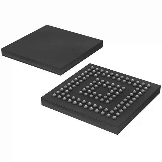
The 113-VFBGA (Microstar Junior 7x7 mm) brings out 74 general-purpose I/O pins, a 16-channel 12-bit ADC, and two 12-bit DACs. The 0.50 mm ball pitch demands a 4-layer PCB with microvias for fan-out — two-layer boards will not route the inner rows of the BGA. The internal oscillator saves an external crystal for most applications; the DCO locks to the USB clock if needed.
Texas Instruments has marked the MSP430F5336IZQWR as obsolete. A board spin is required for a pin-compatible alternative — no drop-in replacement exists in the MSP430F5xx family with the same 113-BGA footprint and peripheral set.