128 KB flash, 10 KB RAM — the real memory envelope
The MSP430F5328IZXH carries 128 KB of program flash (128K x 8) and 10 KB of SRAM. The 16-bit MSP430 CPUXV2 core runs at 25 MHz, but the flash controller inserts wait states above ~8 MHz — the actual instruction throughput is gated by the bus, not the core clock. For a firmware engineer stepping through the boot ROM: the flash prefetch buffer helps, but tight loops with branch-heavy code will stall. The 10 KB RAM split is shared between the stack, heap, and DMA buffers. If your application uses the 12-channel 12-bit SAR ADC for continuous scanning, budget at least 2 KB for the DMA ping-pong buffers alone. The remaining 8 KB must hold the RTOS kernel objects, task stacks, and any large data structures — tight for a TCP/IP stack or GUI framebuffer.
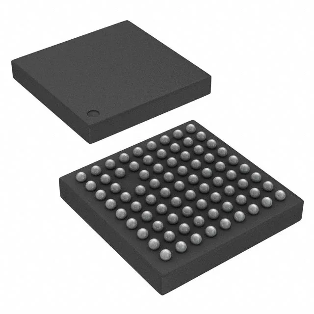
80-NFBGA (5x5) — board layout demands
The 80-NFBGA package measures 5x5 mm with a 0.50 mm ball pitch. This is not a two-layer breakout part — the inner rows of balls require at least a four-layer stack with microvias or blind vias to escape the BGA footprint. The supplier device package is 80-NFBGA (5x5), and the mounting type is surface mount only. If the reflow profile exceeds the floor life, a pre-bake at 125 °C for 48 hours is standard practice before rework. The tray packaging means the parts arrive in a single matrix — no reel, so pick-and-place requires a tray feeder or a bulk-tube adapter.
Industrial temperature and supply voltage envelope
The brown-out detect/reset (BOD) and POR circuits are integrated peripherals — no external supervisor needed for basic power-fail handling. The DMA controller offloads the CPU for ADC data transfers and memory-to-memory moves, which matters when the core is busy servicing the UART/USART or SPI interrupts.
Active production — sourcing posture
The base product number is MSP430F5328, and the series is MSP430F5xx. If a pin-compatible alternative is needed for a second-source hedge, TI's own MSP430F5xx family includes devices with different flash/RAM splits in the same 80-NFBGA footprint — but no official cross-reference is recorded here. Confirm the specific memory and peripheral requirements before substituting.