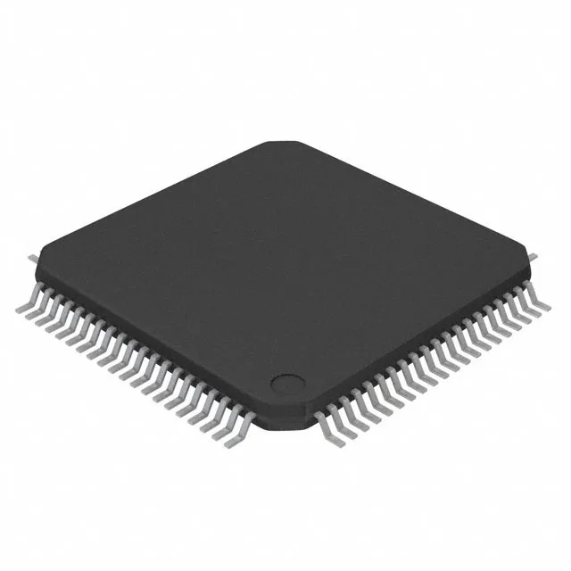
The MSP430F5327IPNR is a 16-bit MCU from the MSP430F5xx family, built around the MSP430 CPUXV2 core clocked at 25 MHz. That clock speed sets the throughput ceiling for control loops and data processing — enough for real-time sensor fusion or motor commutation without an external co-processor. On-chip memory: 96 KB of flash and 8 KB of RAM. The 16-channel 12-bit ADC lets you sample multiple analog inputs without an external multiplexer — handy for a multi-sensor acquisition board.
Package and rework reality
Pin 1 is clearly marked by a chamfer on the moulded body, so you won't play 'where is pin 1?' under the microscope. The exposed pad on the bottom is not a thermal pad for this package; it's just the mould compound base, so no special soldering profile is needed beyond standard LQFP reflow. Surface-mount only — no through-hole variant. The 80-LQFP footprint is common enough that most PCB fab houses have the stencil aperture data ready. No BGA underfill or X-ray inspection required; a visual check under a loupe catches most solder-bridge defects.
63 general-purpose I/O lines give plenty of headroom for parallel displays, keypad matrices, or external memory interfaces. On-chip peripherals include brown-out detect, POR, a watchdog timer, PWM channels, and DMA — the DMA can move ADC results to RAM without CPU intervention, freeing the core for other tasks. Serial connectivity covers UART/USART, SPI, I²C, LINbus, and IrDA. That means one chip can talk to a CAN transceiver (via UART), an SPI flash, an I²C temperature sensor, and a LIN actuator on the same bus without external level shifters.
Lifecycle and sourcing posture
Sourced through independent distribution channels. The 80-LQFP package is widely stocked by TI's distribution network, so lead times are typically manageable for volume orders.