Core architecture and memory map
The MSP430F5253IZQE is a 16-bit MCU built around the MSP430 CPUXV2 core, clocked at 25 MHz — the speed ceiling for this family, which sets the instruction throughput for real-time control loops and data processing tasks. On-chip memory comprises 128 KB of Flash program memory (128K x 8) and 16 KB of RAM (16K x 8), a split that supports moderate-sized firmware images with enough working memory for buffered sensor or communication stacks.
Package and board-fit considerations
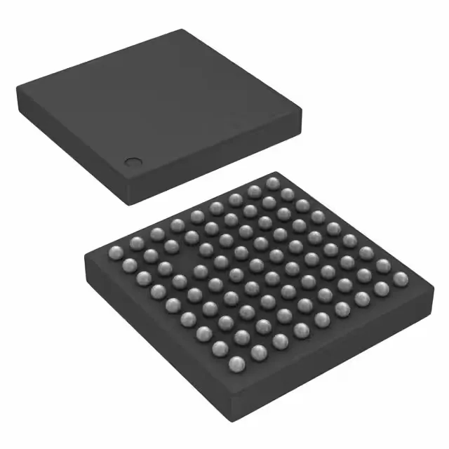
Housed in an 80-VFBGA (MICROSTAR JUNIOR) package measuring 5x5 mm, the MSP430F5253IZQE demands a 4-layer PCB for fan-out of the 0.50 mm pitch BGA balls — the inner rows require microvias or staggered via-in-pad to route all 53 I/O signals.
Temperature grade and deployment envelope
On-chip peripherals include a 10-channel 10-bit ADC, brown-out reset, DMA, POR, PWM, and a watchdog timer — enough on-chip integration to run a sensor node or a small motor-control loop without external analog components.
Lifecycle reality and sourcing posture
Sourced through independent distribution channels; quantities are lot-specific and confirmed at RFQ. No pin-compatible drop-in replacement exists from TI — a board spin is required for any alternative.