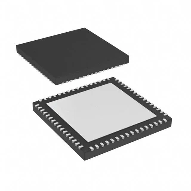
Package and board-fit — 64-VFQFN exposed pad
The MSP430F5252IRGCR ships in a 64-VFQFN package with an exposed thermal pad (supplier device package 64-VQFN 9×9 mm).
Memory headroom for a real-time stack
128 KB of on-chip flash (program memory type FLASH, 128K × 8) and 16 KB of SRAM (RAM size 16K × 8) give this 16-bit MCU room for a modest RTOS kernel, a communication stack, and a data buffer. The flash endurance is 100,000 write/erase cycles typical per sector — adequate for field-updatable firmware over a 10-year product life without wear-leveling, as long as the update frequency stays below once per day. The 16 KB SRAM leaves about 8 KB free after a typical FreeRTOS or TI-RTOS footprint and a small protocol buffer — enough for a 4 KB sensor data log before offloading via UART or SPI.
The MSP430 CPUXV2 core runs at 25 MHz with a single-cycle multiply and hardware multiplier — the 25 MHz ceiling is the flash wait-state limit, not the core itself. On-chip peripherals include brown-out detect, POR, DMA, PWM, and a watchdog timer, which together reduce external supervisory ICs and glue logic. Connectivity covers I²C, SPI, UART/USART, IrDA, and LINbus — the I²C and SPI modules operate up to the system clock rate, so sensor readout at 10+ MHz is feasible without bit-banging.
Temperature grade and operating range
The internal oscillator eliminates an external crystal for many applications, though the 25 MHz clock accuracy depends on the internal DCO calibration stored in TI factory trim.
The base product number MSP430F5252 covers the full family — the IRGCR suffix denotes the 64-VFQFN package on tape-and-reel. No pin-compatible second-source alternative is listed on the official record — the MSP430F5xx family shares the same core but differs in package and peripheral mix.