16-bit core at 25 MHz — what the clock buys you
The MSP430F5249IRGCT: The MSP430 CPUXV2 is a 16-bit RISC core with a hardware multiplier, and the 25 MHz clock is the instruction-cycle ceiling. Real throughput lands lower because flash wait states add cycles above ~8 MHz — the exact number depends on the supply voltage and temperature. For a sensor node polling a 10-bit ADC channel at 200 ksps and logging to flash, the DMA engine (listed among the peripherals) keeps the core sleeping between samples, so the 25 MHz headroom is only tapped during burst processing.
128 KB flash, 8 KB RAM — sizing the BOM
128 KB of program flash and 8 KB of SRAM place this MSP430F5xx variant in the mid-range of the family. The flash holds a full protocol stack (say, a Modbus RTU slave with a 2 KB bootloader) plus the application code, leaving roughly 40 KB free. The 8 KB RAM is the tighter resource — a 2 KB DMA buffer for UART reception plus a 1 KB stack leaves 5 KB for sensor data arrays. If your application needs to buffer a full Ethernet frame or a large LCD frame buffer, step up to the 16 KB RAM variants in the same package.
Peripheral set — what connects, what does not
The connectivity block includes I²C, SPI, UART/USART, and IrDA — enough for a typical sensor hub talking to an external EEPROM, an ADC, and a radio module over SPI. There is no on-chip USB, CAN, or Ethernet MAC; those require an external bridge chip. The 12-channel 10-bit ADC is adequate for reading thermistors, potentiometers, and battery voltage dividers, but not for precision analog loops that need 12+ bits. The brown-out detect (BOR) resets the core if the supply dips below the threshold, which prevents flash corruption during a slow battery discharge.
Package and temperature grade
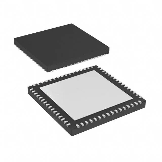
Housed in a 64-VFQFN with an exposed pad (9×9 mm body), the MSP430F5249IRGCT requires a thermal via array under the pad for the -40 to 85 °C industrial range. The 53 I/O lines are all 5 V-tolerant on the digital pins, so level translation is not needed for legacy 5 V peripherals.