Core architecture and memory budget
The MSP430F5229IYFFR runs a 16-bit MSP430 CPUXV2 core at 25 MHz — the instruction set is optimized for low-power control loops, not number crunching, so the 128 KB of on-chip flash and 8 KB of RAM are sized for firmware that spends most of its time in sleep-wake cycles. Program memory is FLASH type with 128 KB (128K x 8) capacity; the 8K x 8 RAM handles the runtime stack and small data buffers typical of sensor fusion or human-machine interface tasks.
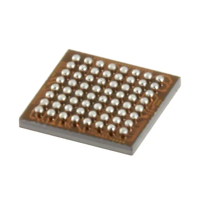
Housed in a 64-ball DSBGA (supplier device package 64-DSBGA), this is a fine-pitch wafer-level package with no leads — the solder balls are the only interface. MSL rating and reflow profile must be verified before the first build; a DSBGA of this density typically requires a stencil aperture matched to the ball diameter and a nitrogen reflow environment to minimize solder ball voiding. The package is surface-mount only, and the 31 I/O plus power balls fan out under the die — expect a 4-layer PCB minimum to route the signals cleanly without via congestion under the package shadow.
The 12-channel 10-bit ADC samples analog inputs without an external converter, though the 10-bit resolution limits precision to 0.1 % of full scale. On-chip peripherals include brown-out detect/reset, DMA, POR, PWM, and a watchdog timer — the brown-out reset ensures the core starts cleanly after a supply dip, critical in battery-powered designs where the rail sags under load.
Production status and sourcing posture
The base product number MSP430F5229 covers the family variants — verify the suffix (IYFFR) matches the required temperature range and package.