Active production — current lifecycle status
The MSP430F5171IYFFR: The part is not subject to allocation or obsolescence risk at this time.
Core architecture and memory budget
Built around the MSP430 CPUXV2 16-bit core running at 25 MHz, this MCU delivers enough throughput for sensor fusion, motor control loops, and real-time communication stacks without the overhead of a 32-bit core. 32 KB of on-chip Flash (32K x 8) provides program storage for moderate-complexity firmware, while 2 KB of RAM (2K x 8) supports data buffering and stack operations.
Package and board integration — 40-DSBGA
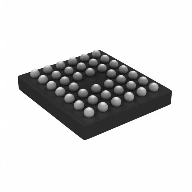
Housed in a 40-ball DSBGA (0.5 mm pitch, 0.4 mm ball diameter), the MSP430F5171IYFFR occupies roughly 3.6 mm × 3.6 mm of board area — about half the footprint of a comparable LQFP-48. The DSBGA package requires careful solder-paste stencil design and X-ray inspection post-reflow, but the trade-off is a significantly smaller board outline compared to a QFN or TSSOP. The 31 I/O lines are distributed across the ball array, so layout must account for fan-out on a 4-layer PCB to avoid routing congestion. Surface-mount assembly with the Tape & Reel packaging supports high-volume pick-and-place.
On-chip peripherals include a brown-out detect/reset (BOR), power-on reset (POR), DMA controller, PWM timers, and a watchdog timer (WDT) — all standard for the MSP430F5xx family. The DMA offloads data transfers from the CPU, which is useful for ADC sampling or UART buffering without stalling the core. Serial connectivity covers I²C, SPI, UART/USART, IrDA, and SCI — enough to interface with most common sensors, radios, and external memory devices.
The part is RoHS-compliant as standard for TI's current portfolio.