25 MHz CPUXV2 — what it means for loop timing
The MSP430F5171IRSBT: The 25 MHz clock drives the CPUXV2 core and integrated peripherals—DMA, PWM, and brown-out reset—without cycle stealing.
32 KB of Flash (32K x 8) and 2 KB of RAM (2K x 8) define the firmware and data footprint this part can hold. The Flash is enough for a moderate application stack—bootloader, communication drivers, calibration tables, and a state-machine control loop—but leaves little room for a full RTOS or extensive GUI library. The 2 KB RAM is the tighter constraint: it handles a few hundred bytes of stack, a modest frame buffer, and DMA buffers, but designs with large look-up tables or extensive packet buffering will need to use Flash for constants and page-swap data. This memory profile aligns with the MSP430F5xx value-tier positioning: enough for the job, not overprovisioned for the cost target.
Supply range and power rail design
At the low end, 1.8 V operation is useful for energy-harvesting or coin-cell designs where every millivolt of headroom extends run time. The integrated brown-out reset (BOR) and power-on reset (POR) supervise the rail, so an external supervisor IC is not needed for most applications.
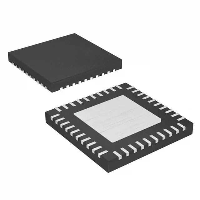
Package and thermal interface: 40-WQFN (5x5 mm)
The 40-WQFN (5x5 mm) with exposed pad is the compact land-grid footprint for this MCU. The 31 I/O lines are distributed around the QFN perimeter.
For a production BOM, this removes the single-source risk that comes with NRND or EOL parts. If a backup is needed, the MSP430F5xx family includes several 40-pin QFN variants with similar peripheral sets, but pin compatibility should be verified against the specific package and I/O mapping.