The 25 MHz clock, combined with the 16-bit RISC architecture, delivers deterministic instruction execution for time-critical tasks like PWM generation and ADC-triggered responses. Memory is tight: 8 KB of Flash for program storage and 1 KB of SRAM. That constrains the firmware to compact state machines, bootloaders, or single-purpose sensor nodes. If your application needs a TCP/IP stack, a GUI library, or data logging beyond a few hundred samples, this part will run out of room. It is sized for a focused task — a motor hall-effect decoder, a battery monitor, a key-fob RF interface — not a general-purpose embedded computer.
40-DSBGA — the assembly reality
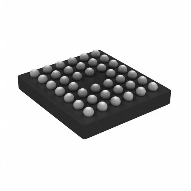
The 40-DSBGA package is a fine-pitch, 0.4 mm or 0.5 mm ball array (TI's DSBGA). This is a reflow-only package — no hand-soldering, no hot-air rework without a stencil and a proper profile. The PCB layout needs a solder-mask-defined pad, via-in-pad for the center balls, and a stencil aperture matched to the ball diameter. If your assembly line is set up for QFP or QFN, this part adds a BGA process step. The reward is a compact footprint — about 2.5 mm × 2.5 mm — for space-constrained designs like wearable sensors or compact modules.
Peripheral set — what is on-chip
The DMA engine can move ADC results to memory without CPU intervention, which helps keep the 25 MHz core free for control math.
Lifecycle status — no LTB risk
TI lists the MSP430F5132IYFFT as Active. The MSP430F5xx series has broad market adoption, and TI typically supports these parts for a decade or more after introduction. ROHS3 compliance is confirmed — no exemptions for lead in solder or other restricted substances. That simplifies EU and California regulatory filings.