Active production, no LTB shadow
ROHS3 compliant per the listing, which matches current EU exemption rules.
The MSP430 CPUXV2 is a 16-bit RISC core rated for 25 MHz operation. At that clock, a single-cycle multiply-accumulate runs in 40 ns, which keeps sensor fusion loops or PID updates inside a 100 µs control period without needing a DMA assist.
8 KB Flash: firmware footprint reality
Program memory is 8 KB of Flash (8K x 8). That is a comfortable fit for a single-purpose controller — a BLDC motor commutation loop, a temperature sensor node with Modbus RTU, or a keypad scanner with I²C display. It will not hold a full Bluetooth stack or a file system. The Flash is field-reprogrammable via the internal bootloader or a debugger, so firmware updates are possible without a dedicated programmer.
40-DSBGA: footprint and layout considerations
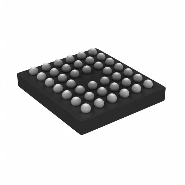
Housed in a 40-ball DSBGA (0.4 mm pitch typical for this class), the MSP430F5131IYFFT saves board area but demands a controlled solder-paste stencil and X-ray inspection after reflow. The 31 I/O lines are accessible through the BGA balls — enough for a parallel LCD bus, a row-column key matrix, and a couple of serial peripherals. Supply decoupling should follow the recommended 0.1 µF per Vcc ball pair, placed directly under the package on the opposite side of the board.
Industrial temperature and peripheral mix
The peripheral set includes brown-out detect, POR, PWM, WDT, and a DMA controller — plus I²C, IrDA, SCI, SPI, and UART/USART connectivity.
The wide range also lets the MCU run directly from a Li-ion cell (3.0 V to 4.2 V) without a series regulator, though the 1.8 V minimum means a boost converter is needed if the battery drops below that threshold. Quiescent current is not specified in the listing, but the MSP430 family is known for sub-1 µA standby modes — expect similar here with careful clock gating.