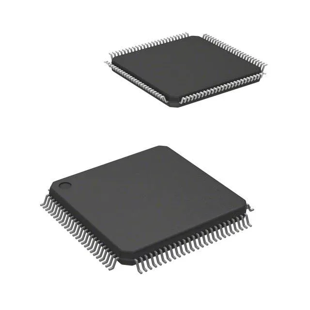
Core and memory budget for instrumentation firmware
The MSP430F4351IPZR runs the 16-bit MSP430 CPU16 at 8 MHz — the clock ceiling sets the instruction throughput for the application loop, and the 16-bit data path matches the register width for efficient 16-bit arithmetic without padding overhead. On-chip memory is 16 KB of FLASH (16K x 8 plus 256 B) and 512 x 8 of RAM — the flash holds the firmware image and constant tables; the RAM budget covers the stack, global variables, and a small data buffer. For a metering or display application that streams data to an LCD, the 512 B RAM is the tightest constraint — the LCD frame buffer and the SPI transmit buffer must share this space.
Peripheral set and serial interface options
Integrated peripherals include a brown-out detect and POR for safe power-up sequencing, a PWM timer for waveform generation, a watchdog timer for runaway-code recovery, and an LCD controller — the LCD controller is the distinguishing feature of the MSP430x4xx family, driving segmented glass displays directly without an external driver chip. Serial connectivity covers SPI and UART/USART — SPI handles high-speed sensor or display data; UART provides a debug console or Modbus RTU link. The 48 general-purpose I/O lines give enough headroom for a keypad matrix, status LEDs, and external memory chip selects alongside the serial buses.
Supply rail, temperature grade, and package footprint
The internal oscillator eliminates the external crystal for the core clock, saving two pins and a PCB trace pair.
Lifecycle and sourcing posture
No pin-compatible second source is documented in the TI portfolio — the MSP430F4351IPZR is a single-source item for the 100-LQFP package with integrated LCD controller.