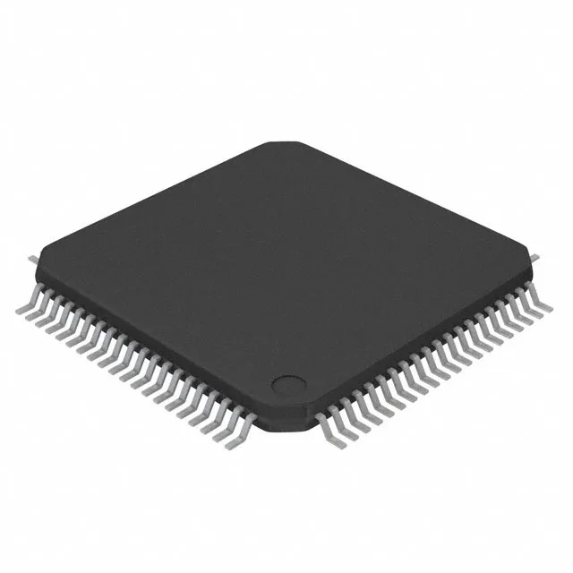
The MSP430F2618TPN: The 16 MHz clock on the MSP430 CPU16 core is the throughput ceiling for this 16-bit architecture. In practice, that translates to about 16 MIPS — enough for real-time control loops, sensor fusion at a few kilohertz, or protocol handling for I2C, SPI, and UART without a separate communications coprocessor. The MSP430's von-Neumann memory architecture means Flash access at 16 MHz requires zero wait states up to 8 MHz; above that the CPU inserts a single wait state per fetch, which the datasheet's instruction-cycle timings already account for. If your interrupt latency budget is tight, the DMA controller (listed among the peripherals) can move ADC results to RAM without CPU involvement, keeping the core free for the main loop.
The Flash is organized as 116 KB plus a separate 256-byte information memory segment that survives a mass erase — useful for calibration constants or MAC addresses that need to persist across firmware updates. The 8 KB RAM is the hard limit for stack, heap, and volatile data buffers. If your application uses a real-time OS or does heavy string manipulation, budget the RAM early; the 64 I/O pins can drive parallel LCDs or memory-mapped peripherals that eat into that space quickly. The integrated DMA helps by offloading peripheral-to-memory transfers without stacking data in the CPU register file.
On-chip analog — ADC and DAC without external converters
The dual DACs can drive analog setpoints for a motor controller or a programmable reference for an external comparator. The 12-bit resolution is adequate for most industrial signal chains; if you need 16 bits, you'd step up to the MSP430F5xx series with a higher-resolution ADC.
Package and temperature range — fits industrial enclosures
The 80-LQFP package (12x12 mm body) gives you 64 usable I/O in a fine-pitch (0.5 mm) surface-mount footprint. That's enough pins to bring out all the serial interfaces (I2C, SPI, UART, LIN, IrDA) plus a parallel data bus for an external memory or display, with headroom for general-purpose GPIO.