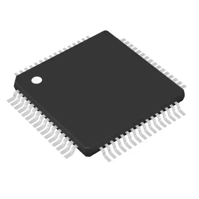
It runs at 16 MHz and packs 8 KB of Flash program memory with 1 KB of RAM, plus an 8-channel 12-bit ADC, a brown-out reset, POR, PWM timer, and a watchdog timer. The 64-pin LQFP package brings out 48 I/O lines.
The 16 MHz clock is the ceiling for instruction throughput on this 16-bit RISC core. In practice, that means a single-cycle multiply completes in 62.5 ns, and the ADC sample-and-hold can trigger every 200 ns or so depending on the clock divider. For a typical PID loop reading one analog channel, computing the correction, and updating a PWM duty cycle, you have roughly 10–15 µs of headroom at 16 MHz — enough for a 10 kHz control rate with margin. If your application needs faster math (FFT, digital filtering at audio rates), you step up to the MSP430F5xx or a Cortex-M0 part. But for 1–10 kHz sensor loops with moderate code complexity, this clock speed is well matched to the Flash access time and avoids wait-state tuning.
The 8 KB program memory (8 K × 8 plus 256 bytes of information memory) is the hard limit for compiled code. A typical bootloader, ADC driver, serial protocol stack, and a modest state machine fit in about 4–5 KB, leaving 3 KB for application logic. The 1 KB RAM (1 K × 8) is the working memory — enough for a few hundred sensor readings, a small circular buffer, and stack. If your firmware exceeds 8 KB, consider the MSP430F2418 (16 KB Flash) or MSP430F2618 (32 KB Flash) in the same package family. The 256-byte information memory is useful for calibration constants and configuration parameters that survive a firmware update.
8-channel 12-bit ADC — analog integration without external parts
The on-chip ADC is a 12-bit successive-approximation converter with 8 multiplexed channels. It samples at up to 200 ksps (typical) and includes an internal voltage reference. For a 3.3 V supply, the LSB is about 805 µV — adequate for 0–10 V sensor outputs after a resistive divider, or for direct battery monitoring. The 12-bit resolution is enough for 0.1% accuracy in most industrial sensor applications (temperature, pressure, level). If you need 16-bit or differential inputs, an external ADC like the ADS1115 would be added; but for single-ended 0–3.6 V signals, this ADC saves a converter chip and the associated routing.
The wide supply range means the MSP430F233TPMR can run directly from two alkaline cells (nominal 3.0 V, dropping to 1.8 V at end of life) or from a regulated 3.3 V rail. At 1.8 V the maximum clock speed is limited — the datasheet specifies 16 MHz only above 2.2 V typical; below that the core slows to 8 MHz or less. For a battery-powered design, you would clock at 1–4 MHz in active mode and use the five low-power modes (LPM0–LPM4) to drop current to sub-µA levels. The 1.8 V minimum also allows direct interface with 1.8 V logic peripherals without level shifters.
The 105°C upper limit covers the under-hood vicinity in passenger vehicles (though not direct engine-bay exposure) and industrial enclosures near motors or power supplies. The 64-LQFP package has a junction-to-ambient thermal resistance around 40–50°C/W, so at 105°C ambient the die stays within the 125°C absolute maximum junction temperature even with all I/O active.