32 KB flash, 1 KB RAM — what fits and what doesn't
The MSP430F2274IYFFR carries 32 KB of program flash and 1 KB of SRAM. That 1 KB RAM is the hard constraint: a sensor fusion stack with a real-time OS, a Bluetooth LE stack, and a 1 kHz control loop will overflow before the flash fills. This part is sized for a single-threaded bare-metal application — a thermistor read, a PID loop, and a UART log.
16 MHz core — what it buys you in a battery node
The 16 MHz clock ceiling is the MSP430 CPU16's sweet spot. At that speed the core draws roughly 360 µA in active mode (typical at 3 V, from the family datasheet). The real power win is the wake-from-sleep latency: the MSP430 exits LPM3 in under 6 µs, so you can burst a calculation at 16 MHz and drop back to 1 µA standby without wasting energy on a warm-up phase. The internal oscillator eliminates the external crystal for the main clock, saving two pins and a PCB trace. For applications requiring a real-time clock, the MSP430F2274 includes a separate 32 kHz watch-crystal oscillator input — the DSBGA package routes those pins to the edge, not the centre, so the crystal can sit close to the die.
Supply voltage and temperature — single-cell battery readiness
No external LDO is needed if the battery sits within this window — the internal POR and brown-out reset (BOR) hold the core in reset below 1.8 V, preventing flash corruption on a dying cell. The DSBGA package's thermal resistance (RθJA ~ 110 °C/W for a 2x2 mm pad) means self-heating at 360 µA active draw is negligible — the die temperature tracks the ambient.
Serial connectivity and ADC — what the peripheral set covers
The IrDA and LINbus support are niche but available — LINbus is useful for automotive body-electronics gateways where this MCU acts as a slave node. The 12-channel 10-bit ADC samples at up to 200 ksps (from the family datasheet). Ten bits is enough for a 0-10 V thermistor read with a 10 mV resolution, but insufficient for a load-cell bridge requiring 16-bit precision. The ADC's reference can be the internal 1.5 V or the supply rail — using Vcc as reference saves a pin but couples supply noise into the measurement.
Active lifecycle — no end-of-life risk for current designs
The MSP430F2xx series has been in production for over a decade with a mature toolchain (CCS, IAR, GCC) and a published errata document — the silicon bugs are known and documented, not discovered mid-production.
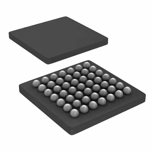
The 49-ball DSBGA (2.8 x 2.8 mm) is a wafer-level chip-scale package. The 0.4 mm ball pitch requires a PCB with micro-vias and a soldermask-defined pad — a two-layer board will struggle to fan out the centre balls. The package is moisture-sensitive (MSL-1 typical for this family), so no bake is needed before reflow if the bag seal is intact.